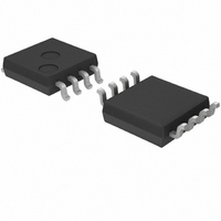
BD9850FVM-TR Rohm Semiconductor, BD9850FVM-TR Datasheet - Page 12

BD9850FVM-TR
Manufacturer Part Number
BD9850FVM-TR
Description
IC REG SW STEP DOWN HI EFF 8MSOP
Manufacturer
Rohm Semiconductor
Type
Step-Down (Buck)r
Series
-r
Datasheet
1.BD9850FVM-TR.pdf
(17 pages)
Specifications of BD9850FVM-TR
Internal Switch(s)
No
Synchronous Rectifier
No
Number Of Outputs
1
Current - Output
200mA
Frequency - Switching
100kHz ~ 2MHz
Voltage - Input
4 ~ 9 V
Operating Temperature
-40°C ~ 85°C
Mounting Type
Surface Mount
Package / Case
8-MSOP, Micro8™, 8-uMAX, 8-uSOP,
Power - Output
587mW
Mounting Style
SMD/SMT
Pwm Type
Controller
Frequency - Max
2MHz
Duty Cycle
-
Voltage - Supply
4 V ~ 9 V
Buck
Yes
Boost
No
Flyback
No
Inverting
No
Doubler
No
Divider
No
Cuk
No
Isolated
No
Lead Free Status / RoHS Status
Lead free / RoHS Compliant
Voltage - Output
-
Lead Free Status / Rohs Status
Lead free / RoHS Compliant
Available stocks
Company
Part Number
Manufacturer
Quantity
Price
Company:
Part Number:
BD9850FVM-TR
Manufacturer:
ST
Quantity:
110
Part Number:
BD9850FVM-TR
Manufacturer:
ROHM/罗姆
Quantity:
20 000
Step-down
Vo2
2PIN(OUT)
6PIN(FB)
(BD9850FVM)
Vcc
(BD9850FVM)
Application circuit / Directions for pattern layout
Equivalent circuit
Vo
200k
20p
Fig.24 Step-down/Step-up application
250k
1µF
C1
C2
10
1
2
3
4
5
6
7
8
9
*
*
SEL1
RT
CT
NON2
INV2
FB2
DTC2
PVCC2
OUT2
PGND
Vcc
OUT
GND
V
REF
PVcc1
OUT
GND
DTC1
OUT1
Vcc
GND
INV1
VCC
V
SCP
Vcc
FB
GND
STB
FB1
REF
20
19
18
17
16
15
14
13
12
11
CTL/SS
INV
RT
FB
4PIN(V
7PIN(CTL/SS)
Fig.26 Equivalent circuit (BD9850FVM)
Fig.23 BD9850FVM Reference application
1.67k
CTL/SS
REF
GND
Vcc
)
*
R1
200k
193k
50k
Step-down
20k
Vo1
12/16
STB
Vcc
GND
[
Vo2
Inverting
ON/OFF
H : OFF
L :ON
5k
]
OUT
GND
Vcc
V
GND
REF
Fig.25 Step-up/Inverting application
Vcc
C1
C1
V
REF
5PIN(INV)
8PIN( R T )
10
1
2
3
4
5
6
7
8
9
Vcc
OUT
GND
V
SEL1
RT
CT
NON2
INV2
FB2
DTC2
PVcc2
OUT2
PGND
REF
C1:
C2:
R1:
500k
GND
In order to reduce ripple noises, set the shortest
distance between the V
and the GND pin and the capacitor pin. Furthermore,
the OUT line may pass under the C1.
In order to reduce ripple noises, set the shortest
pattern between the V
and the GND pin and the capacitor pin.
In order to stabilize the switching frequency, set the
smallest pattern area so that PCB parasitic
capacitance for the RT pin will be minimized.
Vcc
INV
PVcc1
DTC1
OUT1
GND
INV1
V
SCP
STB
FB1
Vcc
REF
20
19
18
17
16
15
14
13
12
11
CT/SS
INV
RT
FB
RT
REF
1k
100k
CC
pin and the capacitor pin,
pin and the capacitor pin,
R1
V
RT
GND
REF
Step-up
VO1
STB
Vcc
GND


