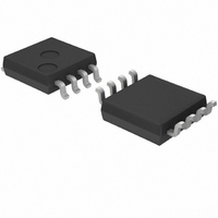
BD9763FVM-TR Rohm Semiconductor, BD9763FVM-TR Datasheet

BD9763FVM-TR
Specifications of BD9763FVM-TR
Available stocks
Related parts for BD9763FVM-TR
BD9763FVM-TR Summary of contents
Page 1
... Single-output Step-up,High-efficiency Switching Regulator (Controller Type) BD9763FVM ●Description BD9763FVM is a 1-channel high efficiency step-up switching regulator possible to choose small application space due to its high-speed operation (Max switching frequency 1.2MHz) ●Features 1) Build-in under voltage lock out circuit. 2) High accuracy reference voltage (2.5V±1.0%) 3) Establish maximum duty cycle internally ...
Page 2
... BD9763FVM ●Electrical characteristics (Unless otherwise specified, Ta=25℃, Vcc=7.0V) Parameter 【Oscillator】 Oscillating frequency Frequency tolerance Swing voltage 【Stand-by, Soft start】 CTL/SS pin source current CTL/SS pin clamp voltage CTL threshold voltage 【PWM comparator】 0% threshold voltage Maximum duty cycle 【 ...
Page 3
... BD9763FVM ●Reference data (Unless otherwise specified, Ta=25℃) VREF voltage vs. Ambient temperature 2.53 2.52 2.51 2.5 2.49 2.48 2.47 -60 -40 - Ambient temperature [℃] Fig.1 VREF voltage – Ambient temperature Oscillating frequency vs. Ambient temperature 650 640 RT=24kΩ 630 ...
Page 4
... BD9763FVM ●Pin configuration 1pin 2pin 3pin 4pin ●Pin number , Pin name Pin No ●Block description ・VOLTAGE REFERENCE(VREF) BLOCK This voltage reference block generates 2.5V internal reference voltage. ・OSCILLATOR BLOCK Oscillator block sets the oscillating frequency adjusted by an external resistance in RT pin. The oscillating frequency can be set within a range of 100~1200kHz.. (See the description of how to set the frequency on page6.) ・ ...
Page 5
... BD9763FVM ●Application example VOUT VCC ●Selecting application components (1) Output inductor It is recommended to use an inductor which satisfies the following rating current (the following value of current), and also has low DCR. The shield type inductor is preferable. I peak = Io・(Vo/VIN) / η + VIN・(VOUT-VIN) / (2・VOUT・L・f) [ Output Vo : Output voltage VIN : Input voltage η ...
Page 6
... BD9763FVM (5) Setting the oscillator frequency Refer to Fig.5 and determine Timing resistor (RRT) when setting the oscillating frequency. 10000 1000 100 1 (6) Setting the output voltage The output voltage is calculated by the following equation VINVth・(R1+R2)/R2 [V] R1,R2 : Resistor divider network VINth : Error amp threshold voltage (typ.1V) (but Vo< ...
Page 7
... BD9763FVM ●Recommended board patterns VOUT Lay out by the shortest pattern. Short GNDs at one point as this figure. VCC C1 OUT C1 GND Capacitor terminals have to be close enough to terminals of VCC and GND safe to pass OUT signal line under C1 Capacitor terminals have to be close enough to terminals of VREF and GND. ...
Page 8
... BD9763FVM ●I/O Equivalent Circuit OUT (2) 250k INV (5) VCC INV GND CTL/SS (7) 5k VCC 20k CTL/SS GND www.rohm.com © 2009 ROHM Co., Ltd. All rights reserved. VREF (4) 1.67k VCC 50k OUT 200k GND 193k FB (6) 20p 200k RT (8) 500k 1k Fig.12 8/11 Technical Note ...
Page 9
... BD9763FVM ●Operation Notes (1) Absolute maximum ratings Use of the IC in excess of absolute maximum ratings such as the applied voltage or operating temperature range may result in IC deterioration or damage. Assumptions should not be made regarding the state of the IC(short mode or open mode) when such damage is suffered. A physical safety measure such as fuse should be implemented when use of the special mode where the absolute maximum ratings may be exceeded is anticipated ...
Page 10
... BD9763FVM (11) IC pin input This monolithic IC contains P + isolation and PCB layers between adjacent elements in order to keep them isolated. P/N junctions are formed at the intersection of these P layers with the N layers of other elements to create a variety of parasitic elements. For example, when a resistor and transistor are connected to pins as shown in Fig.14, ○ ...
Page 11
... BD9763FVM ●Ordering part number Part No. Part No. MSOP8 2.9±0.1 (MAX 3.25 include BURR) + 6° 4° −4° 1PIN MARK 0.145 0.475 S +0.05 0.22 –0.04 0.08 S 0.65 www.rohm.com © 2009 ROHM Co., Ltd. All rights reserved Package FVM: MSOP8 <Tape and Reel information> ...
Page 12
No copying or reproduction of this document, in part or in whole, is permitted without the consent of ROHM Co.,Ltd. The content specified herein is subject to change for improvement without notice. The content specified herein is for the purpose ...


