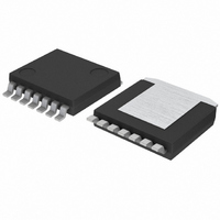
BD9007HFP-TR Rohm Semiconductor, BD9007HFP-TR Datasheet - Page 11

BD9007HFP-TR
Manufacturer Part Number
BD9007HFP-TR
Description
IC REG SW 2A FLEX STEPDOWN HRP7
Manufacturer
Rohm Semiconductor
Type
Step-Down (Buck)r
Series
-r
Datasheet
1.BD9006F-E2.pdf
(18 pages)
Specifications of BD9007HFP-TR
Internal Switch(s)
Yes
Synchronous Rectifier
No
Number Of Outputs
1
Voltage - Output
1 ~ 35 V
Current - Output
2A
Frequency - Switching
50kHz ~ 500kHz
Voltage - Input
7 ~ 35 V
Operating Temperature
-40°C ~ 105°C
Mounting Type
Surface Mount
Package / Case
HRP-7
Power - Output
5.5W
Output Voltage
2. 6 V
Output Current
2 A
Input Voltage
7 V to 35 V
Operating Temperature Range
- 40 C to + 105 C
Mounting Style
SMD/SMT
Duty Cycle (max)
100 %
Lead Free Status / RoHS Status
Lead free / RoHS Compliant
●Directions for pattern layout of PCB
BD9006F, BD9006HFP, BD9007F, BD9007HFP
© 2009 ROHM Co., Ltd. All rights reserved.
4. Selection of diode (D1)
5. Selection of input capacitor (C
6. Setting of oscillating frequenPcy
7. Setting of phase compensation (R3 and C1)
www.rohm.com
Set diode rating with an adequate margin to the
maximum load current. Also, make setting of the rated
inverse voltage with an adequate margin to the
maximum input voltage.
A diode with a low forward voltage and short reverse
recovery time will provide high efficiency.
Two capacitors, ceramic capacitor C
capacitor C28 should be inserted between the V
GND. Be sure to insert a ceramic capacitor of 2 to 10µF
for the C
and a significantly large ripple current. The ripple
current I
If the capacitance of C
may malfunction.
Referring Fig.24 on the following page, select R for the
oscillating frequency to be used.
The phase margin can be set through inserting a capacitor
result.
Select capacitors that can accept this ripple current.
or a capacitor and resistor between the INV pin and the
FB pin. Each set value varies with the output coil,
capacitance, I/O voltage, and load. Therefore, set the
phase compensation to the optimum value according to
these conditions. (For details, refer to Application circuit on
page.11~)
If this setting is not optimum, output oscillation may
※
①
I
RMS
The set values listed above are all reference values. On the actual mounting of the IC, the characteristics may vary with the routing of wirings
and the types of parts in use. In the connection, it is recommended to thoroughly verify these values on the actual system prior to use.
RMS
IN
=Io×
C28
. The capacitor C28 should have a low ESR
can be obtained by the following formula:
⑥
√
C
②
POWER
IN
GND
Vo×(V
Design Method
C1
IN
R3
D1
Fig.24
IN
BD9006HFP
and C28 is not optimum, the IC
L1
-Vo)/V
GND
⑧
C3
IN
IN
, C28)
2
L
O
A
D
R
SIGNAL GND
T
IN
③
R1
R2
and bypass
⑤
⑧
C2
④
IN
and
11/17
Diode ratings must include:
When V
When f=300kHz
From p.11 Fig.24, a resistance of
※Please contact us if there are any questions regarding phase
① Arrange the wirings shown by heavy lines as short as possible in
② Locate the input ceramic capacitor C
③ Locate the R
④ Locate the R1 and R2 as close to the INV pin as possible, and
⑤ Locate the R1 and R2 as far away from the L1 as possible.
⑥ Separate POWER GND (Schottky diode, I/O capacitor’s GND)
⑦ Design the POWER wire line as wide and short as possible.
⑧ Additional pattern for C2 and C3 expand compensation flexibility.
When V
Io=(max.)2A
Current over 2A
Withstand minimum 35V
compensation configuration.
a broad pattern.
pin as possible.
provide the shortest wiring from the R1 and R2 to the INV pin.
and SIGNAL GND (R
effect on SIGNAL GND at all.
IN
IN
=13.2V, Vo=3.3V and Io=1A:
I
(max.)=35V
RMS
=1×
T
as close to the GND pin as possible.
√
3.3×(13.2-3.3)/(13.2)
Sample Calculations
T
, GND), so that SW noise doesn’t have an
R
T
=51kΩ is selected.
IN
as close to the V
I
2
RMS
R
Technical Note
T
2009.05 - Rev.A
=51kΩ
=0.433A
IN
-GND


