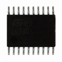
L6730TR STMicroelectronics, L6730TR Datasheet - Page 43

L6730TR
Manufacturer Part Number
L6730TR
Description
IC CTRLR ADJ STEP DOWN 20-TSSOP
Manufacturer
STMicroelectronics
Type
Step-Down (Buck)r
Datasheet
1.L6730TR.pdf
(52 pages)
Specifications of L6730TR
Internal Switch(s)
No
Synchronous Rectifier
Yes
Number Of Outputs
1
Voltage - Output
Adj to 0.6V
Frequency - Switching
100kHz ~ 1MHz
Voltage - Input
1.8 ~ 14 V
Operating Temperature
-40°C ~ 85°C
Mounting Type
Surface Mount
Package / Case
20-TSSOP Exposed Pad, 20-eTSSOP, 20-HTSSOP
Output Voltage
0.6 V
Input Voltage
1.8 V to 14 V
Maximum Operating Temperature
+ 85 C
Minimum Operating Temperature
- 40 C
For Use With
497-5868 - EVAL BOARD 30A 400KHZ L6730497-5501 - EVAL BOARD FOR L6730XX
Lead Free Status / RoHS Status
Lead free / RoHS Compliant
Current - Output
-
Power - Output
-
Lead Free Status / Rohs Status
Lead free / RoHS Compliant
Other names
497-5098-2
Available stocks
Company
Part Number
Manufacturer
Quantity
Price
Part Number:
L6730TR
Manufacturer:
ST
Quantity:
20 000
L6730 - L6730B
8
I/O Description
Figure 38. Demonstration board
Table 11.
Output (V
Input (Vin-Gin)
V
CC
Symbol
V
-GND
TP1
CCDR
OUT
-G
I/O functions
CC
OUT
)
The input voltage can range from 1.8V to 14V. If the input voltage is between
4.5V and 14V it can supply also the device (through the V
case the pin 1 and 2 of the jumper G1 must be connected together.
The output voltage is fixed at 3.3V but it can be changed by replacing the
resistor R14 of the output resistor divider:
The over-current-protection limit is set at 15A but it can be changed by
replacing the resistors R1 and R12 (see OCL and OCH pin in
connection).
Using the input voltage to supply the controller no power is required at this
input. However the controller can be supplied separately from the power stage
through the V
open.
An internal LDO provides the power into the device. The input of this stage is
the V
providing directly a 5V voltage from V
and 3 of the jumper G1 must be shorted.
This pin can be used as an input or as a test point. If all the jumper G2 pins are
shorted, TP1 can be used as a test point of the voltage at the EAREF pin. If
the pins 2 and 3 of G2 are connected together, TP1 can be used as an input to
provide an external reference for the internal error amplifier (see section 4.3.
Internal and external references).
CC
pin and the output (5V) is the V
Doc ID 11938 Rev 3
CC
input (4.5-14V) and, in this case, jumper G1 must be left
Vo
=
V
REF
Function
⋅
CCDR
1 (
CCDR
+
R
R
and Gndcc. In this case the pins 1
16
14
)
pin. The LDO can be bypassed,
CC
pin) and in this
I/O Description
Table 4: Pin
43/52


