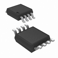
LM3485MM/NOPB National Semiconductor, LM3485MM/NOPB Datasheet - Page 12

LM3485MM/NOPB
Manufacturer Part Number
LM3485MM/NOPB
Description
IC CONTROLLER PFET 8-MSOP
Manufacturer
National Semiconductor
Type
Step-Down (Buck)r
Datasheet
1.LM3485MMNOPB.pdf
(16 pages)
Specifications of LM3485MM/NOPB
Internal Switch(s)
No
Synchronous Rectifier
No
Number Of Outputs
1
Voltage - Output
1.24 ~ 35 V
Current - Output
4A
Voltage - Input
4.5 ~ 35 V
Operating Temperature
-40°C ~ 125°C
Mounting Type
Surface Mount
Package / Case
8-MSOP, Micro8™, 8-uMAX, 8-uSOP,
Power - Output
417mW
Dc To Dc Converter Type
Buck Controller
Pin Count
8
Input Voltage
4.5 to 35V
Output Voltage
1.242 to 35V
Output Current
4A
Package Type
MSOP
Mounting
Surface Mount
Operating Temperature Classification
Automotive
Operating Temperature (min)
-40C
Operating Temperature (max)
125C
For Use With
LM3485LED EVAL - BOARD EVALUATION LM3485LEDLM3485EVAL - BOARD EVALUATION LM3485
Lead Free Status / RoHS Status
Lead free / RoHS Compliant
Frequency - Switching
-
Lead Free Status / Rohs Status
Compliant
Other names
LM3485MM
LM3485MMTR
LM3485MMTR
Available stocks
Company
Part Number
Manufacturer
Quantity
Price
Company:
Part Number:
LM3485MM/NOPB
Manufacturer:
TI
Quantity:
5 600
Part Number:
LM3485MM/NOPB
Manufacturer:
NS/国半
Quantity:
20 000
www.national.com
The off state voltage across the catch diode is approximately
equal to the input voltage. The peak reverse voltage rating
must be greater than input voltage. In nearly all cases a
Schottky diode is recommended. In low output voltage appli-
cations a low forward voltage provides improved efficiency.
For high temperature applications, diode leakage current may
become significant and require a higher reverse voltage rating
to achieve acceptable performance.
P-CHANNEL MOSFET SELECTION (Q1)
The important parameters for the PFET are the maximum
Drain-Source voltage (V
rent rating, and the input capacitance.
The voltage across the PFET when it is turned off is equal to
the sum of the input voltage and the diode forward voltage.
The V
input voltage.
PFET drain current, Id, must be rated higher than the peak
inductor current, I
Depending on operating conditions, the PGATE voltage may
fall as low as V
with a V
As input voltage desreases below 9V, PGATE swing voltage
may also decrease. At 5.0V input the PGATE will swing from
V
and completely, a low threshold PFET should be used when
the input voltage is less than 7V.
However, PFET switching losses will increase as the V
threshold decreases. Therefore, whenever possible, a high
threshold PFET should be selected. Total power loss in the
FET can be approximated using the following equation:
where:
A PFET should be selected with a turn on rise time of less
than 100ns. Slower rise times will degrade efficiency, can
cause false current limiting, and in extreme cases may cause
abnormal spiking at the PGATE pin.
The R
value, R
coefficient. At 100°C, the R
IN
t
t
A value of 10ns to 20ns is typical for ton and toff.
on
off
to V
PDswitch = R
= FET turn on time
= FET turn off time
DS
DSON
GS
IN
ADJ
must be selected to provide some margin beyond the
- 4.6V. To ensure that the PFET turns on quickly
greater than the maximum PGATE swing voltage.
. Note that the R
is used in determining the current limit resistor
IN
- 8.3V. Therefore, a PFET must be selected
IND-PEAK
DSON
*I
DS
OUT
.
), the on resistance (R
2
DSON
DSON
*D + F*I
has a positive temperature
may be as much as 150%
OUT
*V
IN
*(t
on
+ t
DSON
off
)/2
), Cur-
GS
12
higher than the 25°C value. This increase in R
considered it when determining R
range applications. If the current limit is set based upon 25°C
ratings, then false current limiting can occur at high temper-
ature.
Keeping the gate capacitance below 2000pF is recommend-
ed to keep switching losses and transition times low. This will
also help keep the PFET drive current low, which will improve
efficiency and lower the power dissipation within the con-
troller.
As gate capacitance increases, operating frequency should
be reduced and as gate capacitance decreases operating
frequency can be increased.
PCB Layout
The PC board layout is very important in all switching regu-
lator designs. Poor layout can cause switching noise into the
feedback signal and general EMI problems. For minimal in-
ductance, the wires indicated by heavy lines should be as
wide and short as possible. Keep the ground pin of the input
capacitor as close as possible to the anode of the diode. This
path carries a large AC current. The switching node, the node
with the diode cathode, inductor, and FET drain, should be
kept short. This node is one of the main sources for radiated
EMI since it is an AC voltage at the switching frequency. It is
always good practice to use a ground plane in the design,
particularly at high currents.
The two ground pins, PWR GND and GND, should be con-
nected by as short a trace as possible; they can be connected
underneath the device. These pins are resistively connected
internally by approximately 50Ω. The ground pins should be
tied to the ground plane, or to a large ground trace in close
proximity to both the FB divider and C
The gate pin of the external PFET should be located close to
the PGATE pin. However, if a very small FET is used, a re-
sistor may be required between PGATE and the gate of the
FET to reduce high frequency ringing. Since this resistor will
slow the PFET's rise time, the current limit blanking time
should be taken into consideration (see Current Limit Opera-
tion).
The feedback voltage signal line can be sensitive to noise.
Avoid inductive coupling to the inductor or the switching node,
by keeping the FB trace away from these areas.
ADJ
OUT
in wide temperature
grounds.
DSON
must be


