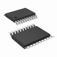
LM25576MH/NOPB National Semiconductor, LM25576MH/NOPB Datasheet - Page 11

LM25576MH/NOPB
Manufacturer Part Number
LM25576MH/NOPB
Description
IC BUCK SYNC ADJ 3A 20TSSOP
Manufacturer
National Semiconductor
Series
PowerWise®, SIMPLE SWITCHER®r
Type
Step-Down (Buck)r
Specifications of LM25576MH/NOPB
Internal Switch(s)
Yes
Synchronous Rectifier
No
Number Of Outputs
1
Voltage - Output
1.23 ~ 40 V
Current - Output
3A
Frequency - Switching
200kHz, 485kHz
Voltage - Input
6 ~ 42 V
Operating Temperature
-40°C ~ 125°C
Mounting Type
Surface Mount
Package / Case
20-TSSOP Exposed Pad, 20-eTSSOP, 20-HTSSOP
Power - Output
4.2W
Current, Input Bias
3.4 mA
Current, Output
3 A
Frequency, Oscillator
50 kHz to 1 MHz
Package Type
TSSOP-20EP
Power Dissipation
1.9 W
Regulator Type
Buck, Switching
Resistance, Thermal, Junction To Case
6 °C/W
Temperature, Operating, Range
-40 to +125 °C
Voltage, Gain
70 dB
Voltage, Input
6 to 42 V
Voltage, Offset
0.7 V
Voltage, Output
7.15 V
Primary Input Voltage
42V
No. Of Outputs
1
Output Voltage
7.45V
Output Current
3A
No. Of Pins
20
Operating Temperature Range
-40°C To +125°C
Msl
MSL 1 - Unlimited
Filter Terminals
SMD
Rohs Compliant
Yes
For Use With
LM25576BLDT - WEBENCH BUILD IT BOARD LM25576LM25576EVAL - BOARD EVALUATION FOR LM25576
Lead Free Status / RoHS Status
Lead free / RoHS Compliant
Other names
*LM25576MH
*LM25576MH/NOPB
LM25576MH
*LM25576MH/NOPB
LM25576MH
Available stocks
Company
Part Number
Manufacturer
Quantity
Price
Part Number:
LM25576MH/NOPB
Manufacturer:
NS/国半
Quantity:
20 000
Error Amplifier and PWM
Comparator
The internal high gain error amplifier generates an error signal
proportional to the difference between the regulated output
voltage and an internal precision reference (1.225V). The
output of the error amplifier is connected to the COMP pin
allowing the user to provide loop compensation components,
generally a type II network, as illustrated in Figure 1. This
network creates a pole at DC, a zero and a noise reducing
high frequency pole. The PWM comparator compares the
emulated current sense signal from the RAMP generator to
the error amplifier output voltage at the COMP pin.
FIGURE 5. Simplified Oscillator Block Diagram and SYNC I/O Circuit
11
RAMP Generator
The ramp signal used in the pulse width modulator for current
mode control is typically derived directly from the buck switch
current. This switch current corresponds to the positive slope
portion of the output inductor current. Using this signal for the
PWM ramp simplifies the control loop transfer function to a
single pole response and provides inherent input voltage
feed-forward compensation. The disadvantage of using the
buck switch current signal for PWM control is the large leading
edge spike due to circuit parasitics that must be filtered or
blanked. Also, the current measurement may introduce sig-
nificant propagation delays. The filtering, blanking time and
propagation delay limit the minimum achievable pulsewidth.
In applications where the input voltage may be relatively large
in comparison to the output voltage, controlling small
pulsewidths and duty cycles is necessary for regulation. The
LM25576 utilizes a unique ramp generator, which does not
actually measure the buck switch current but rather recon-
structs the signal. Reconstructing or emulating the inductor
current provides a ramp signal to the PWM comparator that
is free of leading edge spikes and measurement or filtering
delays. The current reconstruction is comprised of two ele-
ments; a sample & hold DC level and an emulated current
ramp.
20208707
www.national.com


