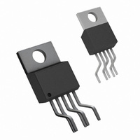
LM2592HVT-ADJ/NOPB National Semiconductor, LM2592HVT-ADJ/NOPB Datasheet - Page 18

LM2592HVT-ADJ/NOPB
Manufacturer Part Number
LM2592HVT-ADJ/NOPB
Description
IC REG SIMPLE SWITCHER TO220-5
Manufacturer
National Semiconductor
Series
SIMPLE SWITCHER®r
Type
Step-Down (Buck)r
Datasheet
1.LM2592HVS-ADJNOPB.pdf
(20 pages)
Specifications of LM2592HVT-ADJ/NOPB
Internal Switch(s)
Yes
Synchronous Rectifier
No
Number Of Outputs
1
Voltage - Output
1.2 ~ 57 V
Current - Output
2A
Frequency - Switching
150kHz
Voltage - Input
4.5 ~ 60 V
Operating Temperature
-40°C ~ 125°C
Mounting Type
Through Hole
Package / Case
TO-220-5 (Bent and Staggered Leads)
Primary Input Voltage
60V
No. Of Outputs
1
Output Voltage
57V
Output Current
2A
No. Of Pins
5
Operating Temperature Range
-40°C To +125°C
Filter Terminals
Through Hole
Rohs Compliant
Yes
Lead Free Status / RoHS Status
Lead free / RoHS Compliant
Power - Output
-
Other names
*LM2592HVT-ADJ
*LM2592HVT-ADJ/NOPB
LM2592HVT-ADJ
*LM2592HVT-ADJ/NOPB
LM2592HVT-ADJ
www.national.com
Application Information
PC board to simulate the junction temperature under actual
operating conditions. This curve can be used for a quick
check for the approximate junction temperature for various
conditions, but be aware that there are many factors that can
affect the junction temperature. When load currents higher
than 2A are used, double sided or multilayer PC boards with
large copper areas and/or airflow might be needed, espe-
cially for high ambient temperatures and high output volt-
ages.
For the best thermal performance, wide copper traces and
generous amounts of printed circuit board copper should be
used in the board layout. (One exception to this is the output
(switch) pin, which should not have large areas of copper.)
Large areas of copper provide the best transfer of heat
(lower thermal resistance) to the surrounding air, and moving
air lowers the thermal resistance even further.
Layout Suggestions
As in any switching regulator, layout is very important. Rap-
idly switching currents associated with wiring inductance can
generate voltage transients which can cause problems. For
minimal inductance and ground loops, with reference to
Figure 1 , the wires indicated by heavy lines should be wide
printed circuit traces and should be kept as short as
possible. For best results, external components should be
located as close to the switcher lC as possible using ground
plane construction or single point grounding.
FIGURE 14. Junction Temperature Rise, TO-263
(Continued)
18
Package thermal resistance and junction temperature rise
numbers are all approximate, and there are many factors
that will affect these numbers. Some of these factors include
board size, shape, thickness, position, location, and even
board temperature. Other factors are, trace width, total
printed circuit copper area, copper thickness, single- or
double-sided, multilayer board and the amount of solder on
the board. The effectiveness of the PC board to dissipate
heat also depends on the size, quantity and spacing of other
components on the board, as well as whether the surround-
ing air is still or moving. Furthermore, some of these com-
ponents such as the catch diode will add heat to the PC
board and the heat can vary as the input voltage changes.
For the inductor, depending on the physical size, type of core
material and the DC resistance, it could either act as a heat
sink taking heat away from the board, or it could add heat to
the board.
If open core inductors are used, special care must be
taken as to the location and positioning of this type of induc-
tor. Allowing the inductor flux to intersect sensitive feedback,
lC groundpath and C
When using the adjustable version, special care must be
taken as to the location of the feedback resistors and the
associated wiring. Physically locate both resistors near the
IC, and route the wiring away from the inductor, especially an
open core type of inductor.
10129438
OUT
wiring can cause problems.


