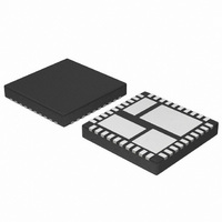
NCP3102MNTXG ON Semiconductor, NCP3102MNTXG Datasheet - Page 9

NCP3102MNTXG
Manufacturer Part Number
NCP3102MNTXG
Description
IC CONV SYNC BUCK 10A 40QFN
Manufacturer
ON Semiconductor
Type
Step-Down (Buck)r
Datasheet
1.NCP3102BMNTXG.pdf
(18 pages)
Specifications of NCP3102MNTXG
Internal Switch(s)
Yes
Synchronous Rectifier
Yes
Number Of Outputs
1
Voltage - Output
Adj to 0.8V
Current - Output
10A
Frequency - Switching
275kHz
Voltage - Input
4.5 ~ 13.2 V
Operating Temperature
0°C ~ 70°C
Mounting Type
Surface Mount
Package / Case
40-TQFN Exposed Pad
Power - Output
3W
Lead Free Status / RoHS Status
Lead free / RoHS Compliant
Other names
NCP3102MNTXGOSTR
transient and sets the duty cycle to maximum, but the current
slope is limited by the inductor value.
drops due to the current variation inside the capacitor and the
ESR. (neglecting the effect of the effective series inductance
(ESL)):
Where V
the effects of ESR and the ESR
series resistance of the output capacitors.
of the NCP3102 demo board with the configuration shown
in Figure 20. The transient response was measured for the
load current step from 5 A to 10 A (50% to 100% load).
OS-CON, output capacitors are 2x100 mF ceramic and
OS-CON as mentioned in Table 1. Typical transient
response waveforms are shown in Figure 17.
at http://www.edc.sanyo.com.
Table 1. TRANSIENT RESPONSE VERSUS OUTPUT
CAPACITANCE
Figure 17. Typical Waveform of Transient Response
C
During a load step transient the output voltage initially
Table 1. shows values of voltage drop and recovery time
Input capacitors are 2x47 mF ceramic and 2x270 mF
More information about OS-CON capacitors is available
OUT
DV
(mF) OS-CON
2x680
2x820
1000
OUT-ESR
100
150
220
270
560
680
820
OUT-ESR
(50% to 100% Load Step)
is the voltage deviation of V
+ DI
Drop (mV)
out
226
182
170
149
112
100
96
71
60
48
ESR
COUT
COUT
Recovery Time (ms)
is the total effective
504
424
264
233
180
180
180
180
284
224
OUT
(eq. 6)
http://onsemi.com
due to
NCP3102
9
current during the load transient without discharging it. The
voltage drop due to the output capacitor discharge is given
by the following equation:
DV
Where V
due to the effects of discharge, L
value and V
Inductor Selection
the selection of an output inductor. From a mechanical
perspective, smaller inductor values generally correspond to
smaller physical size. Since the inductor is often one of the
largest components in the regulation system, a minimum
inductor
space-constrained
perspective, the maximum current slew rate through the
output inductor for a buck regulator is given by:
SlewRate
regulator's ability to slew current through the output
inductor in response to output load transients. Consequently,
output capacitors must supply the load current until the
inductor current reaches the output load current level. This
results in larger values of output capacitance to maintain
tight output voltage regulation. In contrast, smaller values of
inductance increase the regulator's maximum achievable
slew rate and decrease the necessary capacitance, at the
expense of higher ripple current. The peak-to-peak ripple
current is given by the following equation:
Ipk-pk
Where Ipk-pk
From this equation it is clear that the ripple current increases
as L
dynamic response and ripple current. In order to achieve
high efficiency, coils with a low value of Direct Current
Resistance (DCR) have to be used. For example: Coilcraft
MLC1555-302ML and SER2013-362ML).
Feedback and Compensation
shown in Table 2. The adjustment method requires an
external resistor divider with its center tap tied to the FB pin.
It is recommended to have a resistance between 1.5 kW and
5 kW. The selection of low value resistors reduces
efficiency, alternatively high value resistance of R2 causes
decrease in output voltage accuracy due to the bias current
in the error amplifier. The output voltage error of this bias
current can be estimated by using the following equation:
A minimum capacitor value is required to sustain the
Both mechanical and electrical considerations influence
This equation implies that larger inductor values limit the
The output voltage is adjustable from 0.8 V to 5 V as
OUT-DISCHARGE
OUT
LOUT
OUT-DISCHARGE
LOUT
decreases, emphasizing the trade-off between
IN
+
value
LOUT
is the input voltage.
L
+
OUT
V
V
OUT
+
IN
is the peak to peak current of the output.
applications.
L
2
* V
is
( 1 * D )
OUT
275 kHz
is the voltage deviation of V
OUT
C
particularly
OUT
DI
OUT
OUT
V
2
From
IN
is the output inductor
L
OUT
D * V
important
an
OUT
electrical
(eq. 7)
(eq. 8)
(eq. 9)
OUT
in


