LTC3250ES6-1.5#TRM Linear Technology, LTC3250ES6-1.5#TRM Datasheet
LTC3250ES6-1.5#TRM
Specifications of LTC3250ES6-1.5#TRM
Available stocks


Related parts for LTC3250ES6-1.5#TRM


LTC3250ES6-1.5#TRM Summary of contents
Page 1
... The parts are short-circuit and overtemperature protected, and are available in a low profile (1mm) 6-pin TM ThinSOT , LTC and LT are registered trademarks of Linear Technology Corporation Burst Mode is a registered trademark of Linear Technology Corporation ThinSOT is a trademark of Linear Technology Corporation. *U.S. Patent #6, 411, 531 ...
Page 2
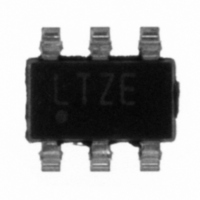
... Junction temperature will exceed 125 C when overtemperature protection is active. Continuous operation above the specified maximum operating junction temperature may impair device reliability ORDER PART NUMBER LTC3250ES6-1 LTC3250ES6-1 OUT – PART MARKING LTZE LTAGJ = 4.7 F unless otherwise noted. OUT MIN TYP ...
Page 3
W U TYPICAL PERFOR A CE CHARACTERISTICS No Load Supply Current vs Supply Voltage 50 3.1V < V < 5.5V (LTC3250-1.5) IN 2.7V < V < 5.5V (LTC3250-1. ...
Page 4
LTC3250-1.5/LTC3250-1 TYPICAL PERFOR A CE CHARACTERISTICS Output Voltage Soft-Start and Shutdown (LTC3250-1.5) HI SHDN LOW V OUT 500mV/DIV 3.6V IN Line Transient Response (LTC3250-1.5) 4. 3.5V V OUT 20mV/DIV AC ...
Page 5
CTIO S V (Pin 1): Input Supply Voltage. Bypass V IN low ESR ceramic capacitor. GND (Pin 2): Ground. Connect to a ground plane for best performance. SHDN (Pin 3): Active Low Shutdown Input. A ...
Page 6
LTC3250-1.5/LTC3250-1.2 U OPERATIO (Refer to Simplified Block Diagram) The LTC3250-1.5/LTC3250-1.2 use a switched capacitor charge pump to step down regulated 1. 1.2V 4% (respectively) output voltage. Regulation is achieved by sensing the output voltage ...
Page 7
U OPERATIO (Refer to Simplified Block Diagram) current. For an ideal step-down charge pump the power efficiency is given by • OUT OUT OUT OUT • ...
Page 8
LTC3250-1.5/LTC3250-1.2 U OPERATIO (Refer to Simplified Block Diagram) Flying Capacitor Selection Warning: A polarized capacitor such as tantalum or aluminum should never be used for the flying capacitor since its voltage can reverse upon start-up of the LTC3250-1.5/LTC3250-1.2. Ceramic capacitors ...
Page 9
U OPERATIO (Refer to Simplified Block Diagram) Thermal Management For higher input voltages and maximum output current there can be substantial power dissipation in the LTC3250-1.5/LTC3250-1.2. If the junction temperature increases above approximately 160 C the thermal shut- down circuitry ...
Page 10
LTC3250-1.5/LTC3250-1.2 U TYPICAL APPLICATIO S Fixed 3.3V Input to 1.5V Output with Shutdown – 3. OUT 1 F LTC3250-1 SHDN GND OFF ON ...
Page 11
... MOLD FLASH SHALL NOT EXCEED 0.254mm 6. JEDEC PACKAGE REFERENCE IS MO-193 Information furnished by Linear Technology Corporation is believed to be accurate and reliable. However, no responsibility is assumed for its use. Linear Technology Corporation makes no represen- tation that the interconnection of its circuits as described herein will not infringe on existing patent rights. LTC3250-1.5/LTC3250-1.2 ...
Page 12
... OUT(MIN) : <1 A, ThinSOT Package SD : 2.5V to 5.5V 0.8V, IN OUT(MIN) : < Package SD : 2.5V to 5.5V 0.8V, IN OUT(MIN) : <1 A, TSSOP16E Package SD : 2.5V to 5.5V 2.5V to 5.5V, IN OUT : < Package SD : 2.4V to 5.5V 2.4V to 5.25V, IN OUT : <1 A, DFN Package SD LT/TP 1203 1K REV A • PRINTED IN USA LINEAR TECHNOLOGY CORPORATION 2001 3250fa ...