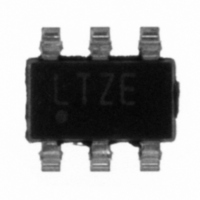
LTC3250ES6-1.5#TRM Linear Technology, LTC3250ES6-1.5#TRM Datasheet - Page 6

LTC3250ES6-1.5#TRM
Manufacturer Part Number
LTC3250ES6-1.5#TRM
Description
IC CONV DC/DC 1.5V S-DWN SOT23-6
Manufacturer
Linear Technology
Type
Step-Down (Buck)r
Datasheet
1.LTC3250ES6-1.5TRM.pdf
(12 pages)
Specifications of LTC3250ES6-1.5#TRM
Internal Switch(s)
Yes
Synchronous Rectifier
No
Number Of Outputs
1
Voltage - Output
1.5V
Current - Output
250mA
Frequency - Switching
1.5MHz
Voltage - Input
3.1 ~ 5.5 V
Operating Temperature
-40°C ~ 85°C
Mounting Type
Surface Mount
Package / Case
SOT-23-6
Lead Free Status / RoHS Status
Contains lead / RoHS non-compliant
Power - Output
-
Other names
LTC3250ES6-1.5#TRMTR
Available stocks
Company
Part Number
Manufacturer
Quantity
Price
OPERATIO
LTC3250-1.5/LTC3250-1.2
6
The LTC3250-1.5/LTC3250-1.2 use a switched capacitor
charge pump to step down V
1.2V 4% (respectively) output voltage. Regulation is
achieved by sensing the output voltage through an internal
resistor divider and modulating the charge pump output
current based on the error signal. A 2-phase nonoverlapping
clock activates the charge pump switches. On the first
phase of the clock current is transferred from V
the flying capacitor, to V
delivered to V
tor is also being charged up. On the second phase of the
clock the flying capacitor is connected from V
ground, delivering the charge stored during the first phase
of the clock to V
half of the output current is delivered from V
achieving twice the efficiency over a conventional LDO.
The sequence of charging and dis-charging the flying
capacitor continues at a free running frequency of 1.5MHz
(typ). This constant frequency architecture provides a low
noise regulated output as well as lower input noise than
conventional switch-capacitor charge pump regulators.
The part also has a low current Burst Mode operation to
improve efficiency even at light loads.
In shutdown mode all circuitry is turned off and the
LTC3250-1.5/LTC3250-1.2 draw only leakage current from
the V
V
voltage of approximately 0.8V. The LTC3250-1.5/LTC3250-
1.2 are in shutdown when a logic low is applied to the
SHDN pin. Since the SHDN pin is a high impedance CMOS
input it should never be allowed to float. To ensure that its
state is defined it must always be driven with a valid logic
level.
Short-Circuit/Thermal Protection
The LTC3250-1.5/LTC3250-1.2 have built-in short-circuit
current limiting as well as overtemperature protection.
During short-circuit conditions, the parts will automati-
cally limit the output current to approximately 500mA. At
higher temperatures, or if the input voltage is high enough
to cause excessive self heating on chip, thermal shutdown
circuitry will shut down the charge pump once the junction
IN
. The SHDN pin is a CMOS input with a threshold
IN
supply. Furthermore, V
OUT
OUT
U
on the first phase, but the flying capaci-
. Using this method of switching, only
(Refer to Simplified Block Diagram)
OUT
IN
. Not only is current being
to a regulated 1.5V 4% or
OUT
is disconnected from
IN
, through
IN
OUT
, thus
to
temperature exceeds approximately 160 C. It will reenable
the charge pump once the junction temperature drops
back to approximately 150 C. The LTC3250-1.5/LTC3250-
1.2 will cycle in and out of thermal shutdown without latch-
up or damage until the short-circuit on V
Long term overstress (I
should be avoided as it can degrade the performance of the
part.
Soft-Start
To prevent excessive current flow at V
the LTC3250-1.5/LTC3250-1.2 have a built-in soft-start
circuitry. Soft-start is achieved by increasing the amount
of current available to the output charge storage capacitor
linearly over a period of approximately 500 s. Soft-start is
enabled whenever the device is brought out of shutdown,
and is disabled shortly after regulation is achieved.
Low Current “Burst Mode” Operation
To improve efficiency at low output currents, Burst Mode
operation was included in the design of the LTC3250-1.5/
LTC3250-1.2. An output current sense is used to detect
when the required output current drops below an inter-
nally set threshold (30mA typ.). When this occurs, the part
shuts down the internal oscillator and goes into a low
current operating state. The LTC3250-1.5/LTC3250-1.2
will remain in the low current operating state until the
output has dropped enough to require another burst of
current. Unlike traditional charge pumps whose burst
current is dependant on many factors (i.e. supply voltage,
switch resistance, capacitor selection, etc.), the LTC3250-
1.5/LTC3250-1.2’s burst current is set by the burst thresh-
old and hysteresis. This means that the V
in Burst Mode will be fixed and is typically 12mV for a
4.7 F output capacitor.
Power Efficiency
The power efficiency ( ) of the LTC3250-1.5/LTC3250-
1.2 are approximately double that of a conventional linear
regulator. This occurs because the input current for a 2 to
1 step-down charge pump is approximately half the output
OUT
> 350mA, and/or T
IN
OUT
OUT
during start-up,
ripple voltage
is removed.
J
> 140 C)
3250fa


