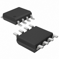
MAX1044CSA+ Maxim Integrated Products, MAX1044CSA+ Datasheet - Page 8

MAX1044CSA+
Manufacturer Part Number
MAX1044CSA+
Description
IC MULTI CONFIG 20MA 8SOIC
Manufacturer
Maxim Integrated Products
Type
Switched Capacitor (Charge Pump), Divider, Doubler, Invertingr
Datasheet
1.MAX1044CSA.pdf
(12 pages)
Specifications of MAX1044CSA+
Internal Switch(s)
Yes
Synchronous Rectifier
No
Number Of Outputs
1
Current - Output
20mA
Frequency - Switching
10kHz
Voltage - Input
1.5 ~ 10 V
Operating Temperature
0°C ~ 70°C
Mounting Type
Surface Mount
Package / Case
8-SOIC (3.9mm Width)
Power - Output
471mW
Output Voltage
- 1.5 V to - 10 V or 3 V to 20 V
Output Current
20 mA
Input Voltage
1.5 V to 10 V
Supply Current
80 uA
Switching Frequency
5 KHz
Mounting Style
SMD/SMT
Maximum Operating Temperature
+ 70 C
Minimum Operating Temperature
0 C
Lead Free Status / RoHS Status
Lead free / RoHS Compliant
Voltage - Output
-
Lead Free Status / Rohs Status
Lead free / RoHS Compliant
a function of oscillator frequency and the capacitor
value. Oscillator frequency, in turn, is influenced by
temperature and supply voltage. For example, with a
5V input voltage and 10µF charge-pump capacitors,
the output resistance is typically 50Ω. Thus, the output
voltage is about -5V under light loads, and decreases
to about -4.5V with a 10mA load current.
Minor supply voltage variations that are inconsequential
to digital circuits can affect some analog circuits.
Therefore, when using the MAX1044/ICL7660 for
powering sensitive analog circuits, the power-supply
rejection ratio of those circuits must be considered.
The output ripple and output drop increase under
heavy loads. If necessary, the MAX1044/ICL7660 out-
put impedance can be reduced by paralleling devices,
increasing the capacitance of C1 and C2, or connect-
ing the MAX1044’s BOOST pin to V+ to increase the
oscillator frequency.
During start-up, pump capacitors C1 and C2 must be
charged. Consequently, the MAX1044/ICL7660 devel-
op inrush currents during start-up. While operating,
short bursts of current are drawn from the supply to C1,
and then from C1 to C2 to replenish the charge drawn
by the load during each charge-pump cycle. If the
voltage converters are being powered by a high-
impedance source, the supply voltage may drop too
low during the current bursts for them to function prop-
erly. Furthermore, if the supply or ground impedance is
too high, or if the traces between the converter IC and
charge-pump capacitors are long or have large loops,
Switched-Capacitor Voltage Converters
Figure 7. External Clocking
8
10µF
_______________________________________________________________________________________
Inrush Current and EMI Considerations
1
2
3
4
MAX1044
ICL7660
8
7
6
5
V+
10k
REQUIRED
FOR TTL
10µF
V
OUT
V+
-(V+)
CMOS or
TTL GATE
switching noise and EMI may be generated. To reduce
these effects:
1) Power the MAX1044/ICL7600 from a low-impedance
2) Add a power-supply bypass capacitor with low
3) Shorten traces between the IC and the charge-pump
4) Arrange the components to keep the ground pins of
5) Leave extra copper on the board around the voltage
The power efficiency of a switched-capacitor voltage
converter is affected by the internal losses in the con-
verter IC, resistive losses of the pump capacitors, and
conversion losses during charge transfer between the
capacitors. The total power loss is:
The internal losses are associated with the IC’s internal
functions such as driving the switches, oscillator, etc.
These losses are affected by operating conditions such
as input voltage, temperature, frequency, and connec-
tions to the LV, BOOST, and OSC pins.
The next two losses are associated with the output
resistance of the voltage converter circuit. Switch losses
occur because of the on-resistances of the MOSFET
switches in the IC. Charge-pump capacitor losses
occur because of their ESR. The relationship between
these losses and the output resistance is as follows:
where:
and f
source.
effective series resistance (ESR) close to the IC
between the V+ and ground pins.
capacitors.
the capacitors and the IC as close as possible.
converter as power and ground planes. This is
easily done on a double-sided PC board.
P
LOSS
OSC
R
OUT
P
PUMP
CAPACITOR
LOSSES
is the oscillator frequency.
= P
INTERNAL
LOSSES
4 2R
(f
OSC
SWITCHES
/ 2) x C1
P
1
+P
SWITCH
LOSSES
Efficiency, Output Ripple,
SWITCH
LOSSES
and Output Impedance
I
+P
OUT
ESR
PUMP
CAPACITOR
LOSSES
2
C1
x R
OUT
ESR
+P
CONVERSION
LOSSES
C2


