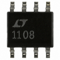
LT1108CS8 Linear Technology, LT1108CS8 Datasheet - Page 10

LT1108CS8
Manufacturer Part Number
LT1108CS8
Description
IC DC/DC CONV ADJUSTBL OUT 8SOIC
Manufacturer
Linear Technology
Type
Step-Down (Buck), Step-Up (Boost), Invertingr
Datasheet
1.LT1108CS8PBF.pdf
(12 pages)
Specifications of LT1108CS8
Internal Switch(s)
Yes
Synchronous Rectifier
No
Number Of Outputs
1
Voltage - Output
Adjustable
Current - Output
400mA
Frequency - Switching
19kHz
Voltage - Input
2 ~ 30 V
Operating Temperature
0°C ~ 70°C
Mounting Type
Surface Mount
Package / Case
8-SOIC (3.9mm Width)
Power - Output
500mW
Lead Free Status / RoHS Status
Contains lead / RoHS non-compliant
Available stocks
Company
Part Number
Manufacturer
Quantity
Price
Part Number:
LT1108CS8
Manufacturer:
LINEAR/凌特
Quantity:
20 000
Part Number:
LT1108CS8#PBF
Manufacturer:
LINEAR/凌特
Quantity:
20 000
Part Number:
LT1108CS8#TRPBF
Manufacturer:
LINEAR/凌特
Quantity:
20 000
Company:
Part Number:
LT1108CS8-12
Manufacturer:
LT
Quantity:
10 000
Part Number:
LT1108CS8-12
Manufacturer:
LINEAR/凌特
Quantity:
20 000
Part Number:
LT1108CS8-12#PBF
Manufacturer:
LINEAR/凌特
Quantity:
20 000
LT1108
A
provided by the PNP transistor, supplies proper polarity
feedback information to the regulator.
–V
USING THE I
The LT1108 switch can be programmed to turn off at a set
switch current, a feature not found on competing devices.
This enables the input to vary over a wide range without
exceeding the maximum switch rating or saturating the
inductor. Consider the case where analysis shows the
LT1108 must operate at an 800mA peak switch current with
a 2.0V input. If V
rise to 1.6A, exceeding the maximum switch current rating.
With the proper resistor selected (see the “Maximum
Switch Current vs R
will be limited to 800mA, even if the input voltage increases.
10
V
IN
PPLICATI
IN
+
+
C2
C2
Figure 4. Positive-to-Negative Converter
Figure 5. Negative-to-Positive Converter
AO
I
LIM
LIM
GND
I
LIM
R3
LT1108
LT1108
IN
PIN
O
GND
V
IN
rises to 4V, the peak switch current will
LIM
U
SW2
V
IN
SW1
SW2
SW1
S
” characteristic), the switch current
FB
FB
L1
I FOR ATIO
U
D1
1N5818
R2
L1
D1
W
+
V
OUT
+
C1
=
R1
R2
C1
1.245V + 0.6V
2N3906
U
R1
R1
R2
LT1108 • F04
–V
LT1108 • F05
V
OUT
OUT
Another situation where the I
when the device goes into continuous mode operation. This
occurs in step-up mode when
When the input and output voltages satisfy this relation-
ship, inductor current does not go to zero during the switch-
OFF time. When the switch turns on again, the current ramp
starts from the non-zero current level in the inductor just
prior to switch turn-on. As shown in Figure 6, the inductor
current increases to a high level before the comparator
turns off the oscillator. This high current can cause exces-
sive output ripple and requires oversizing the output ca-
pacitor and inductor. With the I
switch current turns off at a programmed level as shown in
Figure 7, keeping output ripple to a minimum.
SWITCH
SWITCH
Figure 7. Current Limit Keeps Inductor Current Under Control
V
OUT
OFF
V
OFF
ON
ON
Figure 6. No Current Limit Causes Large Inductor
Current Build-Up
I
IN
I
L
L
PROGRAMMED CURRENT LIMIT
V
V
DIODE
SW
1
1
DC
LIM
.
LIM
feature is useful occurs
feature, however, the
LT1108 • F06
LT1108 • F07
( )
25


