LTC3865EFE#PBF Linear Technology, LTC3865EFE#PBF Datasheet - Page 13
LTC3865EFE#PBF
Manufacturer Part Number
LTC3865EFE#PBF
Description
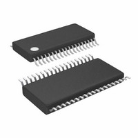
IC BUCK SYNC ADJ DUAL 38TSSOP
Manufacturer
Linear Technology
Type
Step-Down (Buck)r
Datasheet
1.LTC3865EUHPBF.pdf
(38 pages)
Specifications of LTC3865EFE#PBF
Internal Switch(s)
No
Synchronous Rectifier
Yes
Number Of Outputs
2
Voltage - Output
0.6 ~ 5 V
Frequency - Switching
250kHz ~ 770kHz
Voltage - Input
4.5 ~ 38 V
Operating Temperature
-40°C ~ 85°C
Mounting Type
Surface Mount
Package / Case
38-TSSOP Exposed Pad, 38-eTSSOP, 38-HTSSOP
Primary Input Voltage
15V
No. Of Outputs
2
Output Voltage
5V
Output Current
25A
No. Of Pins
38
Operating Temperature Range
-40°C To +85°C
Msl
MSL 1 - Unlimited
Rohs Compliant
Yes
Lead Free Status / RoHS Status
Lead free / RoHS Compliant
Current - Output
-
Power - Output
-
Available stocks
Company
Part Number
Manufacturer
Quantity
Price


OPERATION
pin to a DC voltage below 0.6V (e.g., SGND). To select
pulse-skipping mode of operation, tie the MODE/PLLIN
pin to INTV
MODE/PLLIN pin. When a controller is enabled for Burst
Mode operation, the peak current in the inductor is set to
approximately one-third of the maximum sense voltage
even though the voltage on the I
value. If the average inductor current is higher than the
load current, the error amplifi er EA will decrease the voltage
on the I
internal sleep signal goes high (enabling “sleep” mode)
and both external MOSFETs are turned off.
In sleep mode, the load current is supplied by the output
capacitor. As the output voltage decreases, the EA’s output
begins to rise. When the output voltage drops enough, the
sleep signal goes low, and the controller resumes normal
operation by turning on the top external MOSFET on the
next cycle of the internal oscillator. When a controller is
enabled for Burst Mode operation, the inductor current is
not allowed to reverse. The reverse current comparator
(I
inductor current reaches zero, preventing it from revers-
ing and going negative. Thus, the controller operates in
discontinuous operation. In forced continuous operation,
the inductor current is allowed to reverse at light loads or
under large transient conditions. The peak inductor cur-
rent is determined by the voltage on the I
in normal operation. In this mode, the effi ciency at light
loads is lower than in Burst Mode operation. However,
continuous mode has the advantages of lower output
ripple and less interference with audio circuitry.
When the MODE/PLLIN pin is connected to INTV
LTC3865 operates in PWM pulse-skipping mode at light
loads. At very light loads, the current comparator, I
may remain tripped for several cycles and force the external
top MOSFET to stay off for the same number of cycles (i.e.,
skipping pulses). The inductor current is not allowed to
reverse (discontinuous operation). This mode, like forced
continuous operation, exhibits low output ripple as well as
low audio noise and reduced RF interference as compared
to Burst Mode operation. It provides higher low current
effi ciency than forced continuous mode, but not nearly as
high as Burst Mode operation.
REV
) turns off the bottom external MOSFET just before the
TH
pin. When the I
CC
. To select Burst Mode operation, fl oat the
TH
voltage drops below 0.5V, the
TH
pin indicates a lower
TH
pin, just as
CC
, the
CMP
,
Frequency Selection and Phase-Locked Loop
(FREQ and MODE/PLLIN Pins)
The selection of switching frequency is a trade-off between
effi ciency and component size. Low frequency opera-
tion increases effi ciency by reducing MOSFET switching
losses, but requires larger inductance and/or capacitance
to maintain low output ripple voltage. The switching
frequency of the LTC3865’s controllers can be selected
using the FREQ pin. If the MODE/PLLIN pin is not being
driven by an external clock source, the FREQ pin can be
used to program the controller’s operating frequency from
250kHz to 770kHz.
There is a precision 7.5μA current fl ow out of FREQ pin
that user can program the controller’s switching frequency
with a single resistor to SGND. A curve is provided later in
the application section showing the relationship between
the voltage on the FREQ pin and switching frequency.
A phase-locked loop (PLL) is integrated on the LTC3865
to synchronize the internal oscillator to an external clock
source that is connected to the MODE/PLLIN pin. The
controller is operating in forced continuous mode when
it is synchronized.
The PLL loop fi lter network is integrated inside the
LTC3865/LTC3865-1. The phase-locked loop is capable
of locking any frequency within the range of 250kHz to
770kHz. The frequency setting resistor should always be
present to set the controller’s initial switching frequency
before locking to the external clock.
Power Good (PGOOD Pins)
On the LTC3865 (UH32 package), the PGOOD pin is bonded
to the open drains of two individual internal N-channel
MOSFETs. When either V
of the programmed voltage, the PGOOD pin is pulled low.
The PGOOD pin is also pulled low when either RUN pin
is below 1.22V or when the LTC3865 is in the soft-start
or tracking phase. The PGOOD pin will fl ag power good
immediately when both V
of the programmed output voltage window. However,
there is an internal 20μs power bad mask when either
V
OSENSE
goes out the ±10% window. The internal power
LTC3865/LTC3865-1
OSENSE
OSENSE
voltage is not within ±10%
are within the ±10%
13
3865fb
Related parts for LTC3865EFE#PBF
Image
Part Number
Description
Manufacturer
Datasheet
Request
R

Part Number:
Description:
CD ROM LINEARVIEW DATASHEETS
Manufacturer:
Linear Technology

Part Number:
Description:
Standalone Linear Li-Ion Battery Charger with Thermal Regulation in ThinSOT
Manufacturer:
Linear Technology Corporation
Datasheet:
Part Number:
Description:
Low noise, high frequency, 8th order linear phase lowpass filter
Manufacturer:
Linear Technology Corporation
Datasheet:
Part Number:
Description:
Manufacturer:
Linear Technology Corporation
Datasheet:
Part Number:
Description:
Manufacturer:
Linear Technology Corporation
Datasheet:
Part Number:
Description:
Manufacturer:
Linear Technology Corporation
Datasheet:
Part Number:
Description:
Manufacturer:
Linear Technology Corporation
Datasheet:
Part Number:
Description:
Manufacturer:
Linear Technology Corporation
Datasheet:
Part Number:
Description:
Manufacturer:
Linear Technology Corporation
Datasheet:
Part Number:
Description:
Manufacturer:
Linear Technology Corporation
Datasheet:
Part Number:
Description:
Dual and Quad, JFET Input Precision High Speed Op Amps
Manufacturer:
Linear Technology Corporation
Datasheet:
Part Number:
Description:
Manufacturer:
Linear Technology Corporation
Datasheet:
Part Number:
Description:
1, 2, 6 and 8 Channel, 10-Bit Serial I/O Data Acquisition Systems
Manufacturer:
Linear Technology Corporation
Datasheet:
Part Number:
Description:
Manufacturer:
Linear Technology Corporation
Datasheet:
Part Number:
Description:
Universal dual filter building block
Manufacturer:
Linear Technology Corporation
Datasheet: