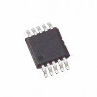
EL7534IYZ Intersil, EL7534IYZ Datasheet - Page 7

EL7534IYZ
Manufacturer Part Number
EL7534IYZ
Description
IC REG 600MA STEP DOWN 10-MSOP
Manufacturer
Intersil
Type
Step-Down (Buck)r
Datasheet
1.EL7534IYZ.pdf
(9 pages)
Specifications of EL7534IYZ
Internal Switch(s)
Yes
Synchronous Rectifier
Yes
Number Of Outputs
1
Voltage - Output
0.8 ~ 5.5 V
Current - Output
600mA
Frequency - Switching
1.5MHz
Voltage - Input
2.5 ~ 5.5 V
Operating Temperature
-40°C ~ 85°C
Mounting Type
Surface Mount
Package / Case
10-MSOP, Micro10™, 10-uMAX, 10-uSOP
Rohs Compliant
YES
Lead Free Status / RoHS Status
Lead free / RoHS Compliant
Power - Output
-
Available stocks
Company
Part Number
Manufacturer
Quantity
Price
Company:
Part Number:
EL7534IYZ
Manufacturer:
Intersil
Quantity:
100
Company:
Part Number:
EL7534IYZ-T13
Manufacturer:
INTERSIL
Quantity:
2 014
Part Number:
EL7534IYZ-T13
Manufacturer:
INTERSIL
Quantity:
20 000
Company:
Part Number:
EL7534IYZ-T7
Manufacturer:
Intersil
Quantity:
1 500
Applications Information
Product Description
The EL7534 is a synchronous, integrated FET 600mA step-
down regulator which operates from an input of 2.5V to 6V.
The output voltage is user-adjustable with a pair of external
resistors.
The internally-compensated controller makes it possible to
use only two ceramic capacitors and one inductor to form a
complete, very small footprint 600mA DC:DC converter.
Start-Up and Shut-Down
When the EN pin is tied to V
approximately 2.4V, the regulator begins to switch. The
output voltage is gradually increased to ensure proper soft-
start operation.
When the EN pin is connected to a logic low, the EL7534 is
in the shut-down mode. All the control circuitry and both
MOSFETs are off, and V
total input current is less than 1µA.
When the EN reaches logic HI, the regulator repeats the
start-up procedure, including the soft-start function.
PWM Operation
In the PWM mode, the P channel MOSFET and N channel
MOSFET always operate complementary. When the
PMOSFET is on and the NMOSFET off, the inductor current
increases linearly. The input energy is transferred to the
output and also stored in the inductor. When the P channel
MOSFET is off and the N channel MOSFET on, the inductor
current decreases linearly, and energy is transferred from
the inductor to the output. Hence, the average current
through the inductor is the output current. Since the inductor
and the output capacitor act as a low pass filter, the duty
cycle ratio is approximately equal to V
The output LC filter has a second order effect. To maintain
the stability of the converter, the overall controller must be
compensated. This is done with the fixed internally
compensated error amplifier and the PWM compensator.
Because the compensations are fixed, the values of input
and output capacitors are 10µF to 22µF ceramic. The
inductor is nominally 1.8µH, though 1.5µA to 2.2µH can be
used.
100% Duty Ratio Operation
EL7534 utilizes CMOS power FET's as the internal
synchronous power switches. The upper switch is a PMOS
and lower switch a NMOS. This not only saves a boot
capacitor, it also allows 100% turn-on of the upper PFET
switch, achieving V
V
V
O
O
is,
=
V
IN
–
(
R
L
+
R
DSON1
O
close to V
OUT
)
×
I
IN
O
falls to zero. In this mode, the
7
, and V
IN
. The maximum achievable
IN
O
reaches
divided by V
IN
.
EL7534
V
Where RL is the DC resistance on the inductor and R
the PFET on-resistance, nominal 70mΩ at room temperature
with tempco of 0.2mΩ/°C.
As the input voltage drops gradually close or even bellow the
preset V
condition, the upper PFET needs some minimum turn-off
time if it is turned off. This off-time is related to input/output
conditions. This makes the duty ratio appears randomly and
increases the output ripple somewhat until the 100% duty
ratio is reached. Larger output capacitor could reduce the
random-looking ripple. Users need to verify if this condition
has adverse effect on overall circuit if close to 100% duty
ratio is expected.
RSI/POR Function
When powering up, the open-collector Power-On-Reset
output holds low for about 100ms after V
preset voltage. When the active-HI reset signal RSI is
issued, POR goes to low immediately and holds for the
same period of time after RSI comes back to LOW. The
output voltage is unaffected. (Please refer to the timing
diagram). When the function is not used, connect RSI to
ground and leave open the pull-up resister R
The POR output also serves as a 100ms delayed Power
Good signal when the pull-up resister R
RSI pin needs to be directly (or indirectly through a resister
R
Output Voltage Selection
Users can set the output voltage of the converter with a
resister divider, which can be chosen based on the following
formula:
Component Selection
Because of the fixed internal compensation, the component
choice is relatively narrow. We recommend 10µF to 22µF
multi-layer ceramic capacitors with X5R or X7R rating for
both the input and output capacitors, and 1.5µH to 2.2µH
inductance for the inductor.
O
6
) connected to Ground for this to function properly.
=
POR
RSI
V
0.8
O
O
×
, the converter gets into 100% duty ratio. At this
FIGURE 14. RSI & POR TIMING DIAGRAM
⎛
⎜
⎝
1
+
R
------ -
R
2
1
⎞
⎟
⎠
100ms
25ns
MIN
4
O
is installed. The
100ms
reaches the
4
at POR pin.
July 12, 2006
DSON1
FN7431.8


