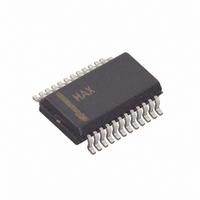
MAX1858AEEG+ Maxim Integrated Products, MAX1858AEEG+ Datasheet - Page 14

MAX1858AEEG+
Manufacturer Part Number
MAX1858AEEG+
Description
IC CNTRLR BUCK DUAL 24-QSOP
Manufacturer
Maxim Integrated Products
Type
Step-Down (Buck)r
Specifications of MAX1858AEEG+
Internal Switch(s)
No
Synchronous Rectifier
No
Number Of Outputs
2
Voltage - Output
0 ~ 18 V
Current - Output
10A
Frequency - Switching
100kHz ~ 600kHz
Voltage - Input
4.5 ~ 23 V
Operating Temperature
-40°C ~ 85°C
Mounting Type
Surface Mount
Package / Case
24-QSOP
Power - Output
762mW
Output Voltage
0 V to 18 V
Output Current
10 A
Input Voltage
4.5 V to 23 V
Mounting Style
SMD/SMT
Maximum Operating Temperature
+ 85 C
Minimum Operating Temperature
- 40 C
Lead Free Status / RoHS Status
Lead free / RoHS Compliant
• SYNC Driven by External Oscillator: The controller
Thermal overload protection limits total power dissipation
in the MAX1858A/MAX1875A/MAX1876A. When the
device’s die-junction temperature exceeds T
an on-chip thermal sensor shuts down the device, forcing
DL_ and DH_ low, allowing the IC to cool. The thermal
sensor turns the part on again after the junction tempera-
ture cools by 10°C. During thermal shutdown, the regula-
tors shut down, RST goes low, and soft-start is reset. If
the V
overload protection is triggered.
Dual 180° Out-of-Phase Buck Controllers with
Sequencing/Prebias Startup and POR
Figure 7. Synchronized Controllers
14
generates the clock signal by dividing down the
SYNC input signal, so that the switching frequency
equals half the synchronization frequency (f
f
ing edge of the internal clock signal. The CKO output
frequency and phase match REG1’s switching fre-
quency (f
phase. Note that the MAX1858A/MAX1875A/
MAX1876A still require R
ly clocked and the internal oscillator frequency should
be set to 50% of the synchronization frequency (f
= 0.5 f
SYNC
______________________________________________________________________________________
L
linear-regulator output is short circuited, thermal-
/2). REG1’s conversion cycles initiate on the ris-
SYNC
MASTER
180° PHASE SHIFT
SLAVE
CKO
OSC
).
MAX1858A
MAX1875A
MAX1876A
MASTER
DH1
DH2
DH
Thermal Overload Protection
= f
3-OUTPUT APPLICATION
DH1
SYNC
CK0
V
) and the CKO signal is in
L
OSC
when SYNC is external-
SYNC
SLAVE
J
= +160°C,
SW
SW
=
Although the MAX1858A/MAX1875A/MAX1876A con-
trollers can operate from input supplies ranging from
4.5V to 23V, the input voltage range can be effectively
limited by the MAX1858A/MAX1875A/MAX1876As’
duty-cycle limitations. The maximum input voltage is
limited by the minimum on-time (t
where t
limited by the switching frequency and minimum off-
time, which determine the maximum duty cycle
(D
where V
in the inductor discharge path, including synchronous
rectifier, inductor, and PC board resistances. V
the sum of the resistances in the charging path, includ-
ing high-side switch, inductor, and PC board resis-
tances.
MAX
OSC
MASTER
V
90° PHASE SHIFT
SLAVE
IN MIN
MAX1858A
MAX1875A
MAX1876A
= 1 - f
MASTER
ON(MIN)
(
DROP1
DH1
DH2
DH1
DH2
)
SW
SYNC
4-OUTPUT APPLICATION
=
CK0
V
is the sum of the parasitic voltage drops
V
⎡
⎢
⎢
⎣
t
is 100ns. The minimum input voltage is
L
IN MAX
1-
OFF(MIN)
V
Effective Input Voltage Range
OUT
(
f
SW OFF MIN
t
+
)
V
≤
):
DROP
SYNC
(
Design Procedure
t
ON MIN SW
MAX1858A
MAX1875A
MAX1876A
1
SLAVE
)
V
(
⎤
⎥
⎥
⎦
OUT
ON(MIN)
+
V
)
f
DROP
OSC
):
2
-
V
DROP
DROP2
1
is


