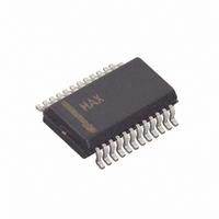
MAX1858AEEG+ Maxim Integrated Products, MAX1858AEEG+ Datasheet - Page 20

MAX1858AEEG+
Manufacturer Part Number
MAX1858AEEG+
Description
IC CNTRLR BUCK DUAL 24-QSOP
Manufacturer
Maxim Integrated Products
Type
Step-Down (Buck)r
Specifications of MAX1858AEEG+
Internal Switch(s)
No
Synchronous Rectifier
No
Number Of Outputs
2
Voltage - Output
0 ~ 18 V
Current - Output
10A
Frequency - Switching
100kHz ~ 600kHz
Voltage - Input
4.5 ~ 23 V
Operating Temperature
-40°C ~ 85°C
Mounting Type
Surface Mount
Package / Case
24-QSOP
Power - Output
762mW
Output Voltage
0 V to 18 V
Output Current
10 A
Input Voltage
4.5 V to 23 V
Mounting Style
SMD/SMT
Maximum Operating Temperature
+ 85 C
Minimum Operating Temperature
- 40 C
Lead Free Status / RoHS Status
Lead free / RoHS Compliant
When working with low input voltages, the output-volt-
age adjustable range for continuous-conduction opera-
tion is restricted by the minimum off-time (t
For best dropout performance, use the lowest (100kHz)
switching-frequency setting. Manufacturing tolerances
and internal propagation delays introduce an error to
the switching frequency and minimum off-time specifi-
cations. This error is more significant at higher frequen-
cies. Also, keep in mind that transient response
performance of buck regulators operated close to
dropout is poor, and bulk output capacitance must
often be added (see the V
Procedure section).
The absolute point of dropout is when the inductor cur-
rent ramps down during the minimum off-time (∆I
as much as it ramps up during the maximum on-time
(∆I
ability to slew the inductor current higher in response to
increased load, and must always be greater than 1. As
h approaches 1, the absolute minimum dropout point,
the inductor current cannot increase as much during
each switching cycle and V
unless additional output capacitance is used.
A reasonable minimum value for h is 1.5, but adjusting
this up or down allows tradeoffs between V
capacitance, and minimum operating voltage. For a
given value of h, the minimum operating voltage can be
calculated as:
where V
in the inductor discharge path, including synchronous
rectifier, inductor, and PC board resistances; V
the sum of the resistances in the charging path, includ-
ing high-side switch, inductor, and PC board resis-
tances; and t
Characteristics. The absolute minimum input voltage is
calculated with h = 1.
If the calculated V+
minimum input voltage, then reduce the operating fre-
quency or add output capacitance to obtain an accept-
able V
calculate V
response.
Dual 180° Out-of-Phase Buck Controllers with
Sequencing/Prebias Startup and POR
20
UP
V
______________________________________________________________________________________
). The ratio h = ∆I
IN MIN
SAG
(
DROP1
. If operation near dropout is anticipated,
)
SAG
=
⎡
⎢
⎢
⎣
is the sum of the parasitic voltage drops
Applications Information
1-
V
OFF(MIN)
OUT
hf
to be sure of adequate transient
SW OFF MIN
(MIN)
+
t
UP
V
DROP
/∆I
is greater than the required
(
SAG
Dropout Performance
DOWN
is from the Electrical
1
)
SAG
⎤
⎥
⎥
⎦
equation in the Design
+
is an indicator of the
V
DROP
greatly increases
2
-
SAG
V
OFF(MIN)
DROP
DROP2
, output
DOWN
1
is
).
)
Dropout design example:
V
f
t
V
h = 1.5
Calculating again with h = 1 gives the absolute limit of
dropout:
Therefore, V
large output capacitance, and a practical input voltage
with reasonable output capacitance would be 6.58V.
Applications where the MAX1858A/MAX1875A/
MAX1876A must operate in noisy environments can
typically adjust their controller’s compensation to
improve the system’s noise immunity. In particular,
high-frequency noise coupled into the feedback loop
causes jittery duty cycles. One solution is to lower the
crossover frequency (see the Compensation section).
Careful PC board layout is critical to achieve low switch-
ing losses and clean, stable operation. This is especially
true for dual converters where one channel can affect
the other. Refer to the MAX1858 EV kit or MAX1875 EV
kit data sheet for specific layout examples.
If possible, mount all the power components on the top
side of the board with their ground terminals flush
against one another. Follow these guidelines for good
PC board layout:
• Isolate the power components on the top side from
SW
OFF(MIN)
OUT
DROP1
the analog components on the bottom side with a
ground shield. Use a separate PGND plane under
the OUT1 and OUT2 sides (referred to as PGND1
and PGND2). Avoid the introduction of AC currents
into the PGND1 and PGND2 ground planes. Run the
power plane ground currents on the top side only.
= 600kHz
= 5V
= V
= 250ns
V
IN MIN
DROP2
V
IN
IN MIN
(
(
must be greater than 6V, even with very
)
=
+
)
= 100mV
PC Board Layout Guidelines
100
=
+
⎡
⎢
⎣
100
1 1 5 600
Improving Noise Immunity
⎡
⎢
⎣
-
1 600
mV
-
. (
(
mV
5
5
−
V
V
100
−
kHz
+
+
100
kHz
100
100
mV
)(
mV
mV
mV
250
)(
=
250
=
6 58
ns
.
6
ns
V
)
⎤
⎥
⎦
V
)
⎤
⎥
⎦


