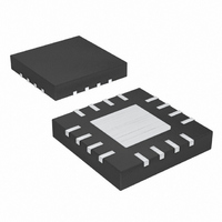
MAX5088ATE+ Maxim Integrated Products, MAX5088ATE+ Datasheet

MAX5088ATE+
Specifications of MAX5088ATE+
Related parts for MAX5088ATE+
MAX5088ATE+ Summary of contents
Page 1
... Integrated 150mΩ High-Side n-Channel Power MOSFET ♦ Power-On Reset Output (MAX5088)/Power-Good Output (MAX5089) ♦ Short-Circuit Protection ♦ Thermal-Shutdown Protection ♦ Thermally Enhanced 16-Pin TQFN Package Dissipates 2.7W PART MAX5088ATE+ MAX5089ATE+ +Denotes lead-free package. Applications TOP VIEW FEATURES RESET Output, BST/VDD Clock Output ...
Page 2
Buck Converters with an Integrated High-Side Switch ABSOLUTE MAXIMUM RATINGS V+ to PGND............................................................-0.3V to +25V BST/VDD, DRAIN to SGND ....................................-0.3V to +30V SGND to PGND .....................................................-0.3V to +0.3V BST/VDD to SOURCE...............................................-0.3V to +6V SOURCE to SGND..................................................-0.6V to +25V ...
Page 3
Buck Converters with an ELECTRICAL CHARACTERISTICS (continued) ( 5.5V to 23V values are +25°C.) (Note PARAMETER SOFT-START Digital Soft-Start Period ...
Page 4
Buck Converters with an Integrated High-Side Switch ELECTRICAL CHARACTERISTICS (continued) ( 5.5V to 23V 5V values are +25°C.) (Note 1) A ...
Page 5
Buck Converters with an ( 5.2V +25°C, Figures 5 and 6, unless otherwise noted MAX5088 BUCK EFFICIENCY vs. OUTPUT CURRENT ( 2.2MHz 3.3V 80 ...
Page 6
Buck Converters with an Integrated High-Side Switch ( 5.2V +25°C, Figures 5 and 6, unless otherwise noted MAX5089 V DROPOUT VOLTAGE L vs. SWITCHING FREQUENCY 0.400 V+ = 5.5V 0.350 0.300 ...
Page 7
Buck Converters with an ( 5.2V +25°C, Figures 5 and 6, unless otherwise noted MAX5089 SOFT-START AND SHUTDOWN (I = 2A) OUT MAX5088/89 toc15 V = 12V IN V 1V/div OUT ...
Page 8
Buck Converters with an Integrated High-Side Switch PIN NAME Internal Power MOSFET Drain Connection. Use the MOSFET as a high-side switch and connect DRAIN to the 1, 2 DRAIN input supply. Transconductance Error Amplifier Output. Connect a compensation ...
Page 9
Buck Converters with an V+ DRAIN SYNC CKO OSCILLATOR OSC 2V 1V BYPASS V REF EN DIGITAL SOFT-START MAX5088 Figure 1. MAX5088 Block Diagram _______________________________________________________________________________________ Integrated High-Side Switch 4-PULSE SKIP ADAPTIVE BBM ...
Page 10
Buck Converters with an Integrated High-Side Switch V+ DRAIN SYNC OSCILLATOR OSC 2V 1V BYPASS V REF EN DIGITAL SOFT-START MAX5089 Figure 2. MAX5089 Block Diagram 10 ______________________________________________________________________________________ 4-PULSE SKIP ADAPTIVE BBM ...
Page 11
Buck Converters with an Detailed Description The MAX5088/MAX5089 use a pulse-width modulation (PWM) voltage-mode control scheme. The MAX5088 is a nonsynchronous converter and uses an external low- forward-drop Schottky diode for rectification. The MAX5089 is a synchronous converter ...
Page 12
Buck Converters with an Integrated High-Side Switch active-high input that turns the MAX5088/ MAX5089 on and off TTL logic input with 2.0V and 0.8V logic-high and low levels, respectively. When EN is ...
Page 13
Buck Converters with an At high input-to-output differential, and high switching frequency, the on-time drops to the order of 100ns. Even though the MAX5088/MAX5089 can control the on-time as low as 100ns, the internal current-limit circuit may not ...
Page 14
Buck Converters with an Integrated High-Side Switch Effective Input Voltage Range The MAX5088/MAX5089 can operate with input sup- plies ranging from 4.5V to 5.5V or 5.5V to 23V. The input voltage range (V+) can be constrained to a ...
Page 15
Buck Converters with an The input ripple comprises mainly of ∆V capacitor discharge) and ∆V (caused by the ESR of ESR the input capacitor). The total voltage ripple is the sum of ∆V and ∆V . Assume the ...
Page 16
Buck Converters with an Integrated High-Side Switch rent through the internal power MOSFET (P The total power dissipated in the package must be lim- ited so the junction temperature does not exceed its absolute maximum rating of +150°C ...
Page 17
Buck Converters with an Calculate the modulator gain (G M quency ESR = × π × V OSC ESR 2 where V is the 1V ramp amplitude and V OSC P-P The ...
Page 18
Buck Converters with an Integrated High-Side Switch V OUT R1 R2 Figure 3. Type II Compensation Network V OUT Figure 4. Type III Compensation Network 18 ______________________________________________________________________________________ REF R ...
Page 19
Buck Converters with an Improving Noise Immunity When using the MAX5088/MAX5089 in noisy environ- ments, adjust the controller’s compensation to improve the system’s noise immunity. In particular, high-fre- quency noise coupled into the feedback loop causes duty-cycle jitter. ...
Page 20
Buck Converters with an Integrated High-Side Switch Figure 5. MAX5088 Buck Configuration 20 ______________________________________________________________________________________ ...
Page 21
Buck Converters with an Figure 6. MAX5089 Buck Configuration ______________________________________________________________________________________ Integrated High-Side Switch 21 ...
Page 22
Buck Converters with an Integrated High-Side Switch SOURCE DUTY CYCLE = 50% SYNC CLKOUT CLKIN MASTER SYNC CLKOUT (MASTER) SOURCE (MASTER) SYNC PHASE SOURCE (SLAVE) CLKOUT Figure 7. Synchronized Converters Pin Configurations (continued) TOP VIEW ...
Page 23
Buck Converters with an (The package drawing(s) in this data sheet may not reflect the most current specifications. For the latest package outline information go to www.maxim-ic.com/packages.) ______________________________________________________________________________________ Integrated High-Side Switch Package Information 23 ...
Page 24
... Maxim cannot assume responsibility for use of any circuitry other than circuitry entirely embodied in a Maxim product. No circuit patent licenses are implied. Maxim reserves the right to change the circuitry and specifications without notice at any time. 24 ____________________Maxim Integrated Products, 120 San Gabriel Drive, Sunnyvale, CA 94086 408-737-7600 © 2006 Maxim Integrated Products Package Information (continued) ...


