MAX5088ATE+ Maxim Integrated Products, MAX5088ATE+ Datasheet - Page 12
MAX5088ATE+
Manufacturer Part Number
MAX5088ATE+
Description
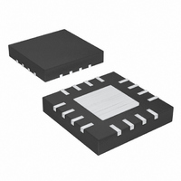
IC DC-DC CONV BUCK 16TQFN
Manufacturer
Maxim Integrated Products
Type
Step-Down (Buck)r
Datasheet
1.MAX5089ATE.pdf
(24 pages)
Specifications of MAX5088ATE+
Internal Switch(s)
Yes
Synchronous Rectifier
No
Number Of Outputs
1
Voltage - Output
0.6 ~ 20 V
Current - Output
2A
Frequency - Switching
200kHz ~ 2.2MHz
Voltage - Input
4.5 ~ 23 V
Operating Temperature
-40°C ~ 125°C
Mounting Type
Surface Mount
Package / Case
16-TQFN Exposed Pad
Power - Output
2.67W
Lead Free Status / RoHS Status
Lead free / RoHS Compliant


EN is an active-high input that turns the MAX5088/
MAX5089 on and off. EN is a TTL logic input with 2.0V
and 0.8V logic-high and low levels, respectively. When
EN is asserted high, the internal digital soft-start cycle
slowly ramps up the internal reference and provides a
soft-start at the output. This hysteresis provides immuni-
ty to the glitches during logic turn-on of the converter.
Voltage variation at EN can interrupt the soft-start
sequence and can cause a latch-up. Ensure that EN
remains high for at least 5ms once it is asserted. Force
EN low to turn off the internal power MOSFET and cause
RESET to pull low (MAX5088) or cause PGOOD to pull
low (MAX5089). Connect EN to V
The MAX5088/MAX5089 include undervoltage lockout
(UVLO) with hysteresis to prevent chattering during
startup. The UVLO circuit holds the MAX5088/MAX5089
off until V+ reaches 4.5V and turns the devices off
when V+ falls below 4.3V. The MAX5088/MAX5089 also
offer a soft-start feature, which reduces surge currents
and glitches on the input during turn-on. During turn-on
when the UVLO threshold is reached or EN goes from
low to high, the digital soft-start ramps up the reference
(V
or V+ low), the reference is reduced to zero slowly. The
soft-start and soft-stop periods (t
the internal oscillator. To calculate the soft-start/soft-
stop period use the following equation:
f
The clock frequency (or switching frequency) is gener-
ated internally and is adjustable through an external
resistor connected from OSC to SGND. The relationship
between R
The adjustment range for f
2.2MHz.
Connect a logic-level clock between 200kHz to 2.2MHz
at SYNC to externally synchronize the MAX5088/
MAX5089’s oscillator (see Figure 7). The MAX5088/
MAX5089 synchronize to the rising edge of the SYNC
clock. The rising edge of the SYNC clock corresponds to
2.2MHz, 2A Buck Converters with an
Integrated High-Side Switch
12
SW
BYPASS
is the switching frequency of the converter.
______________________________________________________________________________________
) in 64 steps. During a turn-off (by pulling EN
OSC
(SYNC)/Clock Output (CLKOUT)
and f
R
OSC
SW
Oscillator/Synchronization
t
SS
=
is:
125 10
=
4096
f
×
SW
f
Soft-Start/Soft-Stop
SW
SW
L
SS
8
when not used.
Ω /
is from 200kHz to
) are 4096 cycles of
s
Enable
the turn-on edge of the internal n-channel power MOSFET
with a fixed propagation delay. When operating the
MAX5088/MAX5089 with an external SYNC clock, R
must be installed. Program the internal switching fre-
quency so that (0.2 x f
minimum pulse width for f
to SGND if synchronization is not used.
The CKO output (MAX5088 only) is a logic-level clock
with the same frequency as f
shift with respect to SYNC clock. Two MAX5088s can
be connected in a master/slave configuration for two-
phase (180°) interleaved operation. The CKO output of
the master drives the SYNC input of the slave to form a
dual-phase converter. To achieve the 180° out-of-phase
operation, program the internal switching frequency of
both converters close to each other by using the same
R
figuration using external clock, program the internal
switching frequency using R
clock frequency (f
(see Figure 7). Any difference in the internal switching
frequency and f
master and slave converters use the same power
source, and share input bypass capacitors, the effec-
tive switching frequency at the input is twice the switch-
ing frequency of the individual converter. Higher ripple
frequency at the input capacitor means a lower RMS
ripple current into the capacitor.
The MAX5088/MAX5089 protect against output over-
load and short-circuit conditions when operated in a
buck configuration. An internal current-sensing stage
develops a voltage proportional to the instantaneous
switch current. When the switch current reaches 2.8A
(typ) the power MOSFET turns off and remains off until
the next on cycle.
During a severe overload or short-circuit condition when
the output voltage is pulled to ground the discharging
slope of the inductor is V
chronous FET), or V
diode) divided by L. The short off-time does not allow
the current to properly ramp down in the inductor, caus-
ing a dangerous current runaway and possibly destruc-
tion of the device. To prevent this, the MAX5088/
MAX5089 include a frequency foldback feature. When
the current limit is detected the frequency is reduced to
1/4th of the programmed switching frequency. When the
output voltage falls below 1/3rd of its nominal set point
(V
cycle is initiated. This reduces the RMS current sourced
by the converter during the fault condition.
OSC
FB
= 0.2V) the converter is turned off and soft-start
value. When synchronizing the master-slave con-
SYNC
SYNC
F
changes the phase delay. If both
(the voltage across the rectifying
SYNC
) for 180° ripple phase operation
DS
SYNC
) ≤ f
(the voltage across the syn-
OSC
SW
is 100ns. Connect SYNC
SW
and with 115° phase
close to the external
≤ (1.2 x f
Current Limit
SYNC
). The
OSC
Related parts for MAX5088ATE+
Image
Part Number
Description
Manufacturer
Datasheet
Request
R

Part Number:
Description:
Voltage-Output, 12-Bit DACs with Internal Reference
Manufacturer:
MAXIM [Maxim Integrated Products]
Datasheet:

Part Number:
Description:
MAX7528KCWPMaxim Integrated Products [CMOS Dual 8-Bit Buffered Multiplying DACs]
Manufacturer:
Maxim Integrated Products
Datasheet:
Part Number:
Description:
Single +5V, fully integrated, 1.25Gbps laser diode driver.
Manufacturer:
Maxim Integrated Products
Datasheet:
Part Number:
Description:
Single +5V, fully integrated, 155Mbps laser diode driver.
Manufacturer:
Maxim Integrated Products
Datasheet:
Part Number:
Description:
VRD11/VRD10, K8 Rev F 2/3/4-Phase PWM Controllers with Integrated Dual MOSFET Drivers
Manufacturer:
Maxim Integrated Products
Datasheet:
Part Number:
Description:
Highly Integrated Level 2 SMBus Battery Chargers
Manufacturer:
Maxim Integrated Products
Datasheet:
Part Number:
Description:
Current Monitor and Accumulator with Integrated Sense Resistor; ; Temperature Range: -40°C to +85°C
Manufacturer:
Maxim Integrated Products
Part Number:
Description:
TSSOP 14/A�/RS-485 Transceivers with Integrated 100O/120O Termination Resis
Manufacturer:
Maxim Integrated Products
Part Number:
Description:
TSSOP 14/A�/RS-485 Transceivers with Integrated 100O/120O Termination Resis
Manufacturer:
Maxim Integrated Products
Part Number:
Description:
QFN 16/A�/AC-DC and DC-DC Peak-Current-Mode Converters with Integrated Step
Manufacturer:
Maxim Integrated Products
Part Number:
Description:
TDFN/A/65V, 1A, 600KHZ, SYNCHRONOUS STEP-DOWN REGULATOR WITH INTEGRATED SWI
Manufacturer:
Maxim Integrated Products
Part Number:
Description:
Integrated Temperature Controller f
Manufacturer:
Maxim Integrated Products
Part Number:
Description:
SOT23-6/I�/45MHz to 650MHz, Integrated IF VCOs with Differential Output
Manufacturer:
Maxim Integrated Products
Part Number:
Description:
SOT23-6/I�/45MHz to 650MHz, Integrated IF VCOs with Differential Output
Manufacturer:
Maxim Integrated Products
Part Number:
Description:
EVALUATION KIT/2.4GHZ TO 2.5GHZ 802.11G/B RF TRANSCEIVER WITH INTEGRATED PA
Manufacturer:
Maxim Integrated Products