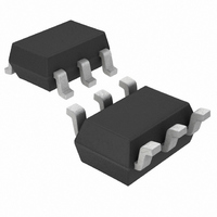
LTC3525ESC6-3#TRPBF Linear Technology, LTC3525ESC6-3#TRPBF Datasheet

LTC3525ESC6-3#TRPBF
Specifications of LTC3525ESC6-3#TRPBF
LTC3525ESC6-3.0#TRPBF
Available stocks
Related parts for LTC3525ESC6-3#TRPBF
LTC3525ESC6-3#TRPBF Summary of contents
Page 1
... The LTC3525 is available in a tiny 6-pin SC70 package. L, LT, LTC, LTM, Burst Mode, Linear Technology and the Linear logo are registered trademarks and ThinSOT is a trademark of Linear Technology Corporation. All other trademarks are the property of their respective owners. Patents pending. ...
Page 2
... Storage Temperature Range .................. –65°C to 125°C Lead Temperature (Soldering, 10 sec) ................... 300°C ORDER INFORMATION LEAD FREE FINISH TAPE AND REEL LTC3525ESC6-3#PBF LTC3525ESC6-3#TRPBF LTC3525ESC6-3.3#PBF LTC3525ESC6-3.3#TRPBF LBTG LTC3525ESC6-5#PBF LTC3525ESC6-5#TRPBF Consult LTC Marketing for parts specified with wider operating temperature ranges. Consult LTC Marketing for information on non-standard lead based finish parts. ...
Page 3
ELECTRICAL CHARACTERISTICS The denotes the specifications which apply over the full operating temperature range, otherwise specifications are 1.2V 1.2V 3.3V unless otherwise noted. IN SHDN OUT PARAMETER Input Start-Up Voltage Output ...
Page 4
LTC3525-3/ LTC3525-3.3/LTC3525-5 TYPICAL PERFORMANCE CHARACTERISTICS Maximum Output Current (for V to Drop 2.5%) OUT 300 LTC3525-3.3 250 200 LTC3525-3 LTC3525-5 150 100 50 0 0.5 1.0 1.5 2.0 2.5 3.0 3.5 4.0 4.5 V (V) IN 3525 ...
Page 5
TYPICAL PERFORMANCE CHARACTERISTICS LTC3525-5 Load Regulation 2 2.4V IN 2.0 1.5 1.0 0 22µF 0 OUT –0.5 –1 10µF OUT –1.5 –2.0 –2 100 120 140 LOAD (mA) 3525 ...
Page 6
LTC3525-3/ LTC3525-3.3/LTC3525-5 TYPICAL PERFORMANCE CHARACTERISTICS LTC3525-3.3 Output Voltage Ripple I OUT 5mA I OUT 40mA I OUT 80mA V = 1.2V 50µs/DIV 22µF OUT LTC3525-5 Output Voltage Ripple I OUT 5mA I OUT 50mA I OUT 150mA ...
Page 7
PIN FUNCTIONS SHDN (Pin 1): Logic-Controlled Shutdown Input. Con- nect to a voltage >1V to enable the LTC3525. Connect to a voltage <0.4V to disable the LTC3525. GND (Pins 2, 5): Ground. V (Pin 3): Input Voltage. The LTC3525 is ...
Page 8
LTC3525-3/ LTC3525-3.3/LTC3525-5 OPERATION The LTC3525 is a high performance Burst Mode operation only, synchronous boost converter requiring only three small external components. Its simplicity and small size make it a high efficiency alternative to charge pump designs designed ...
Page 9
OPERATION which point it turns off and the cycle repeats. When the output voltage reaches its regulated value both switches are turned off and the LTC3525 goes to sleep, during which time the output capacitor supplies current to the load. ...
Page 10
LTC3525-3/ LTC3525-3.3/LTC3525-5 OPERATION Component Selection Inductor values between 4.7µH and 15µH are recom- mended. In most applications 10µH will yield the best compromise between size and efficiency. The inductor should be a low loss ferrite design and must be rated ...
Page 11
TYPICAL APPLICATIONS Single Cell to 3V Converter Using 1mm High Monolithic Inductor 6.8µH* LTC3525 1. SHDN + 2 GND 1µF *FDK MIP3226D6R8M 2-Alkaline or NiMH to 3.3V 10µH* LTC3525-3.3 1. ...
Page 12
LTC3525-3/ LTC3525-3.3/LTC3525-5 PACKAGE DESCRIPTION 0.47 0.65 MAX REF 2.8 BSC 1.8 REF RECOMMENDED SOLDER PAD LAYOUT PER IPC CALCULATOR 0.10 – 0.40 GAUGE PLANE 0.15 BSC 0.26 – 0.46 NOTE: 1. DIMENSIONS ARE IN MILLIMETERS 2. DRAWING NOT TO SCALE ...
Page 13
... Updated “Shutdown” section Information furnished by Linear Technology Corporation is believed to be accurate and reliable. However, no responsibility is assumed for its use. Linear Technology Corporation makes no representa- tion that the interconnection of its circuits as described herein will not infringe on existing patent rights. LTC3525-3/ LTC3525-3 ...
Page 14
... V = 7.5V, I < 1µA, OUT(MAX 1. 6V, I < 1µA, OUT(MAX 1. 10V OUT(MAX) < 1µA, ThinSOT Package : 2.3V to 10V 34V 25µA, OUT(MAX) Q < 1µA, ThinSOT Package LT 0910 REV B • PRINTED IN USA LINEAR TECHNOLOGY CORPORATION 2005 = 10µA, Q 3525fb ...


