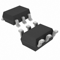
LTC3525ESC6-3#TRPBF Linear Technology, LTC3525ESC6-3#TRPBF Datasheet - Page 9

LTC3525ESC6-3#TRPBF
Manufacturer Part Number
LTC3525ESC6-3#TRPBF
Description
IC DC/DC CONV 3V SC70-6
Manufacturer
Linear Technology
Type
Step-Up (Boost)r
Datasheet
1.LTC3525ESC6-5TRMPBF.pdf
(14 pages)
Specifications of LTC3525ESC6-3#TRPBF
Internal Switch(s)
Yes
Synchronous Rectifier
Yes
Number Of Outputs
1
Voltage - Output
3V
Current - Output
400mA
Voltage - Input
0.85 ~ 4.5 V
Operating Temperature
-40°C ~ 85°C
Mounting Type
Surface Mount
Package / Case
SC-70-6, SC-88, SOT-363
Lead Free Status / RoHS Status
Lead free / RoHS Compliant
Power - Output
-
Frequency - Switching
-
Other names
LTC3525ESC6-3.0#TRPBF
LTC3525ESC6-3.0#TRPBF
LTC3525ESC6-3.0#TRPBF
Available stocks
Company
Part Number
Manufacturer
Quantity
Price
OPERATION
which point it turns off and the cycle repeats. When the
output voltage reaches its regulated value both switches
are turned off and the LTC3525 goes to sleep, during
which time the output capacitor supplies current to the
load. Once the output voltage drops approximately 9mV
below the regulation value the IC leaves sleep mode and
switching is resumed.
The LTC3525 has been designed for low output voltage
ripple. The output voltage ripple is typically only 20mV
peak-to-peak at light load and 60mV peak-to-peak at
full load using the minimum recommended 10µF output
capacitor for the LTC3525-3.3 and a 22µF capacitor for
the LTC3525-5 (due to the capacitor’s DC bias effect). An
antiring circuit damps any oscillation at the switch node
when the inductor current falls to zero.
Power Adjust Feature
The LTC3525 incorporates a feature that maximizes
efficiency at light load while providing increased power
capability at heavy load by adjusting the peak and valley
of the inductor current as a function of load. Lowering the
peak inductor current to 150mA at light load optimizes
efficiency by reducing conduction losses in the internal
MOSFET switches. As the load increases, the peak inductor
current is automatically increased to a maximum of 400mA.
At intermediate loads, the peak inductor current may vary
100mA/DIV
INDUCTOR
Figure 2. Inductor Current Changing as a Function of Load
50mA/DIV
CURRENT
CURRENT
LOAD
10µs/DIV
from 150mA to 400mA. Figure 2 shows an example of
how the inductor current changes as the load increases.
Please note that output capacitor values greater than 47µF
will result in higher peak currents than necessary at light
load. This will lower the light load efficiency.
The valley of the inductor current is automatically adjusted
as well, to maintain a relatively constant inductor ripple
current. This keeps the switching frequency relatively
constant.
The maximum average load current that can be supported
is given by:
where η is the efficiency (see Typical Performance Char-
acteristics).
The “burst” frequency (how often the LTC3525 delivers
a burst of current pulses to the load) is determined by
the internal hysteresis (output voltage ripple), the load
current and the amount of output capacitance. All Burst
Mode operation or hysteretic converters will enter the
audible frequency range when the load is light enough.
However, due to the low peak inductor current at light
load, circuits using the LTC3525 do not typically generate
any audible noise.
I
O MAX
(
LTC3525-3.3/LTC3525-5
)
=
0 3 . •
3525 F02
V
V
O
IN
• η
Amps
LTC3525-3/
3525fb
9


