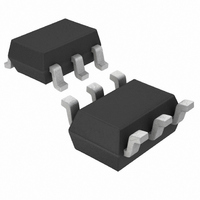
LTC3525LESC6-3#TRMPBF Linear Technology, LTC3525LESC6-3#TRMPBF Datasheet

LTC3525LESC6-3#TRMPBF
Specifications of LTC3525LESC6-3#TRMPBF
Available stocks
Related parts for LTC3525LESC6-3#TRMPBF
LTC3525LESC6-3#TRMPBF Summary of contents
Page 1
... The LTC3525L-3 is available in a tiny 6-pin SC70 package. L, LT, LTC, LTM, Burst Mode, Linear Technology and the Linear logo are registered trademarks and ThinSOT is a trademark of Linear Technology Corporation. All other trademarks are the property of their respective owners. Patents pending. ...
Page 2
... ORDER INFORMATION LEAD FREE FINISH TAPE AND REEL LTC3525LESC6-3#PBF LTC3525LESC6-3#TRPBF LCPY Consult LTC Marketing for parts specified with wider operating temperature ranges. Consult LTC Marketing for information on non-standard lead based finish parts. For more information on lead free part marking, go to: For more information on tape and reel specifications, go to: ...
Page 3
TYPICAL PERFORMANCE CHARACTERISTICS Maximum Output Current (for V to Drop 2.5%) OUT 300 250 200 150 100 50 0 0.5 1.0 1.5 2.0 2.5 V (V) IN 3525L G01 Efficiency and Power Loss vs Load 100 90 ...
Page 4
LTC3525L-3 TYPICAL PERFORMANCE CHARACTERISTICS Input Current and 1. OUT 1V/DIV INPUT CURRENT 100mA/DIV 100µs/DIV Output Voltage Ripple I OUT 5mA I OUT 40mA I OUT 80mA V = 1.2V 50µs/DIV 22µF OUT ...
Page 5
PIN FUNCTIONS SHDN (Pin 1): Logic-Controlled Shutdown Input. Connect to a voltage >0.88V to enable the LTC3525L-3. Connect to a voltage <0.3V to disable the LTC3525L-3. GND (Pins 2, 5): Ground. V (Pin 3): Input Voltage. The LTC3525L-3 is powered ...
Page 6
LTC3525L-3 OPERATION The LTC3525L high performance Burst Mode op- eration only, synchronous boost converter requiring only three small external components. Its simplicity and small size make it a high efficiency alternative to charge pump designs designed ...
Page 7
OPERATION During start-up, the synchronous rectifier is not enabled, and the internal P-channel synchronous rectifier acts as a follower, causing the peak voltage reach (V + 1V) typical. This limits inrush current by maintaining IN control of ...
Page 8
LTC3525L-3 OPERATION The maximum average load current that can be supported is given by: • η 0.3 • Amps ( O MAX V O where η is the efficiency (see Typical Performance Char- acteristics). The ...
Page 9
OPERATION Table 1. Inductor Vendor Information SUPPLIER PHONE Murata USA: (814) 237-1431 Coilcraft (847) 639-6400 Sumida USA: (847) 956-0666 Taiyo Yuden (408) 573-4150 Table 2. Capacitor Vendor Information SUPPLIER PHONE Murata USA: (814) 237-1431 Taiyo Yuden (408) 573-4150 TDK (847) ...
Page 10
LTC3525L-3 PACKAGE DESCRIPTION 0.47 0.65 MAX REF 2.8 BSC 1.8 REF RECOMMENDED SOLDER PAD LAYOUT PER IPC CALCULATOR 0.10 – 0.40 GAUGE PLANE 0.15 BSC 0.26 – 0.46 NOTE: 1. DIMENSIONS ARE IN MILLIMETERS 2. DRAWING NOT TO SCALE 3. ...
Page 11
... Text update to Operations Shutdown Section Added Figure 1 Information furnished by Linear Technology Corporation is believed to be accurate and reliable. However, no responsibility is assumed for its use. Linear Technology Corporation makes no representa- tion that the interconnection of its circuits as described herein will not infringe on existing patent rights. LTC3525L-3 ...
Page 12
... ThinSOT Package : 0.85V to 4.5V 5V, IN OUT(MAX) = 7µA, I < 1µA, SC70 Package SD : 0. 5.25V, IN OUT(MAX) < 1µA, 2mm × 2mm DFN Package = 9µA/300µ 1110 REV A • PRINTED IN USA LINEAR TECHNOLOGY CORPORA TION 2006 V OUT 3V 160mA 10µF = 10µA, Q 3525lfa ...


