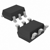
LTC3525LESC6-3#TRMPBF Linear Technology, LTC3525LESC6-3#TRMPBF Datasheet - Page 6

LTC3525LESC6-3#TRMPBF
Manufacturer Part Number
LTC3525LESC6-3#TRMPBF
Description
IC DC/DC CONV 3V SC70-6
Manufacturer
Linear Technology
Type
Step-Up (Boost)r
Datasheet
1.LTC3525LESC6-3TRPBF.pdf
(12 pages)
Specifications of LTC3525LESC6-3#TRMPBF
Internal Switch(s)
Yes
Synchronous Rectifier
Yes
Number Of Outputs
1
Voltage - Output
3V
Current - Output
400mA
Voltage - Input
0.5 ~ 4.5 V
Operating Temperature
-40°C ~ 85°C
Mounting Type
Surface Mount
Package / Case
SC-70-6, SC-88, SOT-363
Lead Free Status / RoHS Status
Lead free / RoHS Compliant
Power - Output
-
Frequency - Switching
-
Available stocks
Company
Part Number
Manufacturer
Quantity
Price
LTC3525L-3
OPERATION
The LTC3525L-3 is a high performance Burst Mode op-
eration only, synchronous boost converter requiring only
three small external components. Its simplicity and small
size make it a high efficiency alternative to charge pump
designs. It is designed to start up from a single alkaline
or nickel cell, with input voltages as low as 0.7V typical
or 0.88V maximum, or from two or three cells (or a Li-Ion
battery), with voltages as high as 4.5V. Once started, V
can be as low as 0.5V (depending on load current) and
maintain regulation. The output voltage is preset internally
to 3V. Peak switch current is 400mA minimum, providing
regulation with load currents up to 160mA, depending on
input voltage.
Synchronous rectification provides high efficiency opera-
tion while eliminating the need for an external Schottky
diode. True output disconnect eliminates inrush current
at start-up, and allows V
for zero shutdown current.
The output disconnect feature also allows the LTC3525L-3
to maintain regulation with an input voltage equal to or
greater than V
rectifier is not enabled in this mode resulting in lower
efficiency and reduced output current capability.
The operating quiescent current is only 7µA typical, allow-
ing the converter to maintain high efficiency at extremely
light loads.
6
OUT
. Note, however, that the synchronous
OUT
Figure 1. Recommended Shutdown Circuits when Driving SHDN Above V
to be disconnected from V
V
CNTRL
R > (V
CNTRL
R
LTC3525L-3
/(V
SHDN
IN
+ 0.4) – 1) M
1M
IN
IN
,
V
CNTRL
V
IN
Shutdown
The LTC3525L-3 is shut down by pulling SHDN below
0.3V, and made active by raising it above 0.88V. Although
SHDN can be driven above V
maximum rating) without damage, the LTC3525L-3 has a
proprietary test mode that may be engaged if SHDN is held
in the range of 0.5V to 1V higher than the greater of V
V
action is interrupted, which can cause undesirable opera-
tion in some applications. Therefore, in applications where
SHDN may be driven above V
means must be employed to keep the SHDN voltage below
(V
being engaged. Please refer to Figure 1 for two possible
implementations.
After the SHDN pin rises, there is a short delay before
switching starts. The delay is 20µs to 120µs, depending
on input voltage (see Typical Performance Characteristics
curve).
Start-Up
A start-up oscillator allows the LTC3525L-3 to start with in-
put voltages as low as 0.7V. It remains in start-up mode until
two conditions are met. V
0.2V typical and either V
1.8V typical.
OUT
IN
ZETEX ZC2811E
. If the test mode is engaged, normal PWM switching
+ 0.4V) to prevent the possibility of the test mode
1M
LTC3525L-3
SHDN
3525L F01
IN
OUT
or V
IN
IN
IN
must exceed V
or V
, a resistor divider or other
OUT
OUT
must be greater than
(up to the absolute
IN
by at least
IN
3525lfa
or


