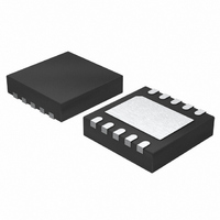
LTC3447EDD Linear Technology, LTC3447EDD Datasheet - Page 6

LTC3447EDD
Manufacturer Part Number
LTC3447EDD
Description
IC CONV DC/DC SYNC BUCK 10DFN
Manufacturer
Linear Technology
Type
Step-Down (Buck)r
Datasheet
1.LTC3447EDDPBF.pdf
(16 pages)
Specifications of LTC3447EDD
Internal Switch(s)
Yes
Synchronous Rectifier
Yes
Number Of Outputs
1
Voltage - Output
0.69 ~ 2.05 V
Current - Output
600mA
Frequency - Switching
1MHz
Voltage - Input
2.5 ~ 5.5 V
Operating Temperature
-40°C ~ 85°C
Mounting Type
Surface Mount
Package / Case
10-DFN
Lead Free Status / RoHS Status
Contains lead / RoHS non-compliant
Power - Output
-
Available stocks
Company
Part Number
Manufacturer
Quantity
Price
Company:
Part Number:
LTC3447EDD
Manufacturer:
LT
Quantity:
10 000
Company:
Part Number:
LTC3447EDD#PBF
Manufacturer:
LT
Quantity:
110
Part Number:
LTC3447EDD#PBF
Manufacturer:
LINEAR/凌特
Quantity:
20 000
Part Number:
LTC3447EDD#TRPBF
Manufacturer:
LINEAR/凌特
Quantity:
20 000
PI FU CTIO S
LTC3447
V
resistor divider provides the divided down feedback refer-
ence for comparison.
GND (Pin 2): Ground for all Circuits Excluding the Internal
Synchronous Power NFET.
FB (Pin 3): Feedback Sensing Pin for the Optional External
Feedback Resistors. Must be tied to V
external feedback resistors.
PGOOD (Pin 4): Fault Report. Open drain driver sinks cur-
rent when V
DAC changes can be enabled via the I
V
to GND with a 2.2µF or greater capacitor.
BLOCK DIAGRA
PGOOD
6
OUT
IN
V
RUN
SDA
SCL
CCD
U
(Pin 5): Main Supply Pin. Must be closely decoupled
(Pin 1): Output Voltage Sensing Pin. An internal
LTC3447
U
POWER
GOOD
BURST
OUT
I
2
C
BLANK
is 10% out of tolerance. Blanking during
6-BIT DAC
REF
UV REF
OV REF
U
LOAD
DAC
W
V
DAC
S
MUX
2
C.
Figure 2. LTC3447 High Level Block Diagram
IN
if there are no
+
–
V
IN
SLEW
SOFT-START
C
IN
SW (Pin 6): Switch Node Connector to Inductor. This pin
connects the drains of the internal main and synchronous
power MOSFET switches.
RUN (Pin 7): Run Control Input. Forcing pin above 1.5V
enables the part. Forcing the pin below 0.3V shuts down
the device. In shutdown, all functions are disabled draw-
ing <1µA of supply current. Do not leave the RUN pin
fl oating.
SCL (Pin 8): I
V
SDA (Pin 10): I
Exposed Pad (Pin 11): Ground. Must be connected to
PCB ground for electrical contact and optimized thermal
performance.
CCD
V
(Pin 9): I
REF
REGULATOR
BURST
BUCK
2
2
C Clock Input.
2
C Power Rail.
C Data Input.
SW
V
FB
MUX
R
DAC
1.3R
3447 BD
SW
FB
R1
R2
V
OUT
C
3447f
OUT


