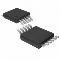
LTC3704IMS#TRPBF Linear Technology, LTC3704IMS#TRPBF Datasheet - Page 13

LTC3704IMS#TRPBF
Manufacturer Part Number
LTC3704IMS#TRPBF
Description
IC INV SYNC 5.2V 50MA 10MSOP
Manufacturer
Linear Technology
Type
Invertingr
Datasheet
1.LTC3704EMSPBF.pdf
(28 pages)
Specifications of LTC3704IMS#TRPBF
Internal Switch(s)
No
Synchronous Rectifier
No
Number Of Outputs
1
Voltage - Output
-5.2V
Current - Output
50mA
Frequency - Switching
50kHz ~ 1MHz
Voltage - Input
2.5 ~ 36 V
Operating Temperature
-40°C ~ 125°C
Mounting Type
Surface Mount
Package / Case
10-MSOP, Micro10™, 10-uMAX, 10-uSOP
Lead Free Status / RoHS Status
Lead free / RoHS Compliant
Power - Output
-
Available stocks
Company
Part Number
Manufacturer
Quantity
Price
APPLICATIO S I FOR ATIO
Applications Circuits
A simple positive-to-negative application circuit for the
LTC3704 is shown in Figure 1. The basic operation of this
circuit is shown in Figure 9. During the on-time the
inductor currents flow through the switch, and during the
off-time these currents flow through the output diode. The
use of inductors in series with both the input and output
results in continuous currents in these capacitors, result-
ing in low input and output noise. Discontinuous currents
flow in the switch, the coupling capacitor, and the diode.
Duty Cycle Considerations
For the positive-to-negative converter shown in Figure 1,
the duty cycle of the main switch in CCM is:
where V
voltage for this converter (in CCM) is:
The maximum duty cycle capability of the LTC3704 is
typically 92%.
D
V
O MAX
=
(
Figure 9. Positive-to-Negative Converter Operation
V
O
O
V
V
IN
IN
V
)
is a negative number. The maximum output
–
OFF
O
ON
=
a) Current Flow During The Switch On-Time
b) Current Flow During The Switch Off-Time
+
+
V
IN
V
IN MIN
(
L1
U
L1
)
+
+
•
1
–
D
U
–
–
L2
MAX
D
MAX
L2
+
+
W
R
R
L
L
3704 F09
V
V
OUT
OUT
U
Peak and Average Input and Switch Currents
The control loop in the LTC3704 is measuring the peak
switch current (either by using the R
MOSFET or by using a sense resistor in the MOSFET
source), so the output current needs to be reflected back
to the switch in order to dimension the power MOSFET and
inductors properly. Based on the fact that, ideally, the
input power is equal to the output power, the maximum
average input current is:
where I
current is:
In a positive-to-negative converter, however, the switch
current is equal to I
current is:
and the peak switch current is:
The maximum duty cycle, D
minimum V
Ripple Current ΔI
The constant ‘ χ ’ in the equation above represents the
percentage peak-to-peak total ripple current in the induc-
tor, relative to its maximum value. For example, if 30%
ripple current is chosen, then χ = 0.30, and the peak
current is 15% greater than the average.
For a current mode converter operating in CCM, slope
compensation must be added for duty cycles above 50%
in order to avoid subharmonic oscillation. For the LTC3704,
this ramp compensation is internal. Having an internally
fixed ramp compensation waveform, however, does place
some constraints on the value of the inductor and the
operating frequency. If too large an inductor is used, the
resulting current ramp (ΔI
I
I
I
I
IN MAX
IN PEAK
SW MAX
SW PEAK
(
(
(
(
O(MAX)
)
)
)
=
)
IN
= − +
= −
= − +
.
–
I
⎛
⎜
⎝
O MAX
is a negative number. The peak input
I
O MAX
1
(
⎛
⎜
⎝
L
(
1
IN
and the ‘ χ ’ Factor
+ I
χ
2
)
χ
2
⎞
⎟
⎠
O
)
•
⎞
⎟
⎠
•
, so the maximum average switch
•
1
I
•
1
O MAX
–
D
I
L
(
−
O MAX
) will be small relative to the
D
MAX
MAX
(
D
MAX
1
MAX
)
, should be calculated at
•
)
•
1
1
–
D
DS(ON)
–
D
MAX
D
MAX
1
MAX
LTC3704
of the power
13
3704fb


