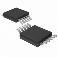
LTC3704IMS#TRPBF Linear Technology, LTC3704IMS#TRPBF Datasheet - Page 17

LTC3704IMS#TRPBF
Manufacturer Part Number
LTC3704IMS#TRPBF
Description
IC INV SYNC 5.2V 50MA 10MSOP
Manufacturer
Linear Technology
Type
Invertingr
Datasheet
1.LTC3704EMSPBF.pdf
(28 pages)
Specifications of LTC3704IMS#TRPBF
Internal Switch(s)
No
Synchronous Rectifier
No
Number Of Outputs
1
Voltage - Output
-5.2V
Current - Output
50mA
Frequency - Switching
50kHz ~ 1MHz
Voltage - Input
2.5 ~ 36 V
Operating Temperature
-40°C ~ 125°C
Mounting Type
Surface Mount
Package / Case
10-MSOP, Micro10™, 10-uMAX, 10-uSOP
Lead Free Status / RoHS Status
Lead free / RoHS Compliant
Power - Output
-
Available stocks
Company
Part Number
Manufacturer
Quantity
Price
APPLICATIO S I FOR ATIO
The R
the R
the case to the ambient temperature (R
of T
used in the iterative calculation process.
Output Diode Selection
To maximize efficiency, a fast switching diode with low
forward drop and low reverse leakage is desired. The
output diode in a positive-to-negative converter conducts
current during the switch off-time. The peak reverse
voltage that the diode must withstand is equal to V
– V
equal to the output current, and the peak current is equal
to the peak inductor current.
The power dissipated by the diode is:
and the diode junction temperature is:
The R
the R
the board to the ambient temperature in the enclosure.
Remember to keep the diode lead lengths short and to
observe proper switch-node layout (see Board Layout
Checklist) to avoid excessive ringing and increased
dissipation.
Selecting the DC Coupling Capacitor
The voltage on the coupling capacitor in a positive-to-
negative converter is V
due to the ripple currents in the inductors. Generally, the
DC coupling capacitor is dimensioned based on the high
RMS ripple which flows in it, as shown in Figure 13.
The minimum RMS current rating of this capacitor must
exceed:
P
T
I
I
O
D PEAK
RMS CAP
J
J
D
. The average forward current in normal operation is
(
TH(JC)
can then be compared to the original, assumed value
TH(JC)
= T
TH(JA)
TH(JA)
= I
(
O(MAX)
A
)
+ P
for the device plus the thermal resistance from
for the device plus the thermal resistance from
=
)
to be used in this equation normally includes
to be used in this equation normally includes
=
–
D
⎛
⎜
⎝
–
• V
• R
1
I
+
O MAX
D
TH(JA)
(
U
χ
2
⎞
⎟
⎠
IN(MAX)
•
)
I
•
O MAX
U
(
1
– V
–
D
)
D
MAX
O
1
MAX
, plus any additional ΔV
–
W
D
1
MAX
TH(CA)
). This value
U
IN(MAX)
A low ESR and ESL, X5R- or X7R-type ceramic capacitor
is recommended here.
Selecting the Output Capacitor
The output ripple voltage appears as a triangular wave-
form riding on V
component of the current in L2 equals the output current).
This ripple current flows through the ESR and bulk capaci-
tance of the output capacitor to produce the overall ripple
voltage on this node. Using the off-time to calculate this
ripple current results in the following equation for ΔI
where V
is therefore:
The ESR can be minimized by using high quality, X5R- or
X7R-dielectric ceramic capacitor in parallel with a larger
value tantalum or aluminum electrolytic bulk capacitor.
Depending upon the application, it may be that the ceramic
capacitor alone will be sufficient.
The RMS ripple current rating of the output capacitor
needs to be greater than:
ΔI
ΔV
⎡
⎢
⎣
–
Figure 13. Ripple Current in the DC Coupling Capacitor
L
1A/DIV
ESR
O P P
2
( – )
O
= –
is a negative number. The output ripple voltage
–
1
8
=
–
• •
1
D
f C
O
1
f
–
MAX
, due to the ripple current of L2 (the DC
D
f
O
MAX
⎤
⎥
⎦
•
V
L
O
2
500ns/DIV
•
V
L
O
2
LTC3704
3704 F13
17
3704fb
L2
:


