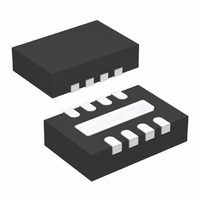
LTC3125EDCB#TRPBF Linear Technology, LTC3125EDCB#TRPBF Datasheet - Page 6

LTC3125EDCB#TRPBF
Manufacturer Part Number
LTC3125EDCB#TRPBF
Description
IC DC/DC CONV STP-UP 1.2A 8-DFN
Manufacturer
Linear Technology
Type
Step-Up (Boost)r
Datasheet
1.LTC3125EDCBTRMPBF.pdf
(18 pages)
Specifications of LTC3125EDCB#TRPBF
Internal Switch(s)
Yes
Synchronous Rectifier
Yes
Number Of Outputs
1
Voltage - Output
2 ~ 5.25 V
Current - Output
1.2A
Frequency - Switching
1.6MHz
Voltage - Input
1.8 ~ 5.5 V
Operating Temperature
-40°C ~ 85°C
Mounting Type
Surface Mount
Package / Case
8-DFN
Lead Free Status / RoHS Status
Lead free / RoHS Compliant
Power - Output
-
Available stocks
Company
Part Number
Manufacturer
Quantity
Price
LTC3125
TYPICAL PERFORMANCE CHARACTERISTICS
PIN FUNCTIONS
GND (Pin 1, Exposed Pad Pin 9): Ground. The exposed
pad must be soldered to the PCB ground plane for electrical
connection and for rated thermal performance.
FB (Pin 2): Feedback Input to the Error Amplifi er. Connect
the resistor divider tap to this pin. The top of the divider
connects to V
to GND. The output voltage can be adjusted from 1.8V
to 5.25V.
PROG (Pin 3): Programming Input for Average Input Cur-
rent. This pin should be connected to ground through an
external resistor (R
threshold. Refer to the Component Selection section in
Applications Information for details on selecting R
V
until V
0.25V), the device is powered from V
bypass capacitor from V
1μF is recommended. Also connects to CS through 60mΩ
internal sense resistor.
6
IN
(Pin 4): Input Voltage. The device is powered from V
OUT
exceeds V
200mA/DIV
CURRENT
OUT
2V/DIV
5V/DIV
INPUT
SHDN
V
OUT
and the bottom of the divider connects
PROG
V
V
C
L = 2.7μH
V
IN
OUT
OUT
OUT
IN
= 3.3V
. Once V
= 4.5V
= 1F
) to set input average current limit
and I
IN
to GND. A minimum value of
IN
During Soft-Start
OUT
2s/DIV
is greater than (V
OUT
. Place a ceramic
3125 G20
PROG
IN
IN
.
+
CS (Pin 5): Current Sense Resistor Connection Point.
Connect the inductor directly to CS. An internal 60mΩ
sense resistor is connected between CS and V
SHDN (Pin 6): Logic Controlled Shutdown Input. Bringing
this pin above 1V enables the part, forcing this pin below
0.35V disables the part.
V
Synchronous Rectifi er. Connect the output fi lter capacitor
from V
150μF is recommended. Due to the output disconnect
feature, V
SW (Pin 8): Switch Pin. Connect an inductor from this
pin to CS. An internal anti-ringing resistor is connected
across SW and CS after the inductor current has dropped
near zero.
OUT
(Pin 7): Output Voltage Sense and the Output of the
OUT
100
90
85
80
70
50
95
75
65
60
55
OUT
Effi ciency vs V
2
(T
I
V
to GND, close to the IC. A minimum value of
LOAD
OUT
A
is disconnected from V
= 25°C unless otherwise noted)
= 3.8V
= 200mA
3
IN
V
IN
(V)
4
IN
3125 G21
when SHDN is low.
5
IN
.
3125fa


