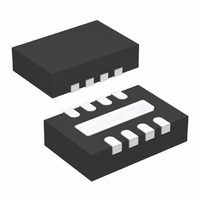
LTC3125EDCB#TRPBF Linear Technology, LTC3125EDCB#TRPBF Datasheet - Page 8

LTC3125EDCB#TRPBF
Manufacturer Part Number
LTC3125EDCB#TRPBF
Description
IC DC/DC CONV STP-UP 1.2A 8-DFN
Manufacturer
Linear Technology
Type
Step-Up (Boost)r
Datasheet
1.LTC3125EDCBTRMPBF.pdf
(18 pages)
Specifications of LTC3125EDCB#TRPBF
Internal Switch(s)
Yes
Synchronous Rectifier
Yes
Number Of Outputs
1
Voltage - Output
2 ~ 5.25 V
Current - Output
1.2A
Frequency - Switching
1.6MHz
Voltage - Input
1.8 ~ 5.5 V
Operating Temperature
-40°C ~ 85°C
Mounting Type
Surface Mount
Package / Case
8-DFN
Lead Free Status / RoHS Status
Lead free / RoHS Compliant
Power - Output
-
Available stocks
Company
Part Number
Manufacturer
Quantity
Price
OPERATION
LTC3125
The LTC3125 provides high effi ciency, low noise power
for applications in portable instrumentation and those
with pulsed-load, power-limited requirements such as
GSM modems.
The LTC3125 directly and accurately controls the average
input current. The high effi ciency of the LTC3125 provides
the maximum possible output current to the load without
impacting the host. Together with an external bulk capaci-
tor the LTC3125 with average input current limit allows a
GSM/GPRS modem to be interfaced directly to a PCMCIA
or CompactFlash power bus without overloading it.
The current mode architecture with adaptive slope com-
pensation provides excellent transient load response,
requiring minimal output fi ltering. Internal soft-start and
loop compensation simplifi es the design process while
minimizing the number of external components.
With its low R
nel MOSFET switch and P-channel MOSFET synchronous
rectifi er, the LTC3125 achieves high effi ciency over a wide
range of load currents. Automatic Burst Mode operation
maintains high effi ciency at very light loads, reducing the
quiescent current to just 15μA.
ERROR AMPLIFIER
The noninverting input of the transconductance error
amplifi er is internally connected to the 1.2V reference
and the inverting input is connected to FB. Clamps limit
the minimum and maximum error amp output voltage for
improved large-signal transient response. Power converter
control loop compensation is provided internally. An exter-
nal resistive voltage divider from V
the output voltage via FB from 2V to 5.25V.
INTERNAL CURRENT LIMIT
Lossless current sensing converts the peak current signal of
the N-channel MOSFET switch into a voltage that is summed
with the internal slope compensation. The summed signal
is compared to the error amplifi er output to provide a peak
current control command for the PWM.
8
V
OUT
=1.2V 1+
DS(ON)
⎛
⎝ ⎜
R2
R1
and low gate charge internal N-chan-
⎞
⎠ ⎟
OUT
to ground programs
A second current limit comparator shuts off the N-chan-
nel MOSFET switch once the peak current signal clamp
threshold is reached. The current limit comparator delay
to output is typically 60ns. Peak switch current is limited
to approximately 1.8A, independent of input or output
voltage, unless V
current limit is cut in half.
AVERAGE INPUT CURRENT LIMIT
A current proportional to the internally sensed input current
is sourced out of the PROG pin. The voltage across the
external resistor on the PROG pin is averaged and com-
pared to a temperature stable internal reference, providing
a signal to actively control the current limit comparator’s
clamp threshold. The high gain of this loop forces the
average input current to the limit set by the value of the
external resistor, R
The LTC3125 is trimmed and tested at 500mA to obtain a
±5% initial accuracy. At other current limit settings, non-
idealities such as random offsets in the input current limit
loop will degrade the accuracy in the application. R
tolerance must also be considered when setting the input
current limit as the accuracies listed in the Electrical Char-
acteristics section do not include external resistor variation.
Traditional, internally compensated, current mode con-
trolled boost converters can be unstable with the high
capacitance and low ESR values used in supercapacitor
chargers and pulsed load applications. The internal loop
compensation of the LTC3125 is optimized to be stable with
output capacitor values greater than 150μF with very low
ESR. Output capacitor values below 150μF will degrade
transient response and can lead to instability.
Note that the LTC3125’s input current averaging circuit
may introduce a slightly higher inductor current ripple
than expected. This is normal and has no affect on the
average input current seen by the power source.
ZERO CURRENT COMPARATOR
The zero current comparator monitors the inductor cur-
rent to the output and shuts off the synchronous rectifi er
when this current reduces to approximately 30mA. This
OUT
PROG
falls below 0.8V, in which case the
.
PROG
3125fa


