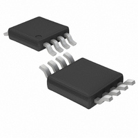
LTC1877EMS8#TR Linear Technology, LTC1877EMS8#TR Datasheet - Page 12

LTC1877EMS8#TR
Manufacturer Part Number
LTC1877EMS8#TR
Description
IC BUCK SYNC ADJ .6A 8MSOP
Manufacturer
Linear Technology
Type
Step-Down (Buck)r
Datasheet
1.LTC1877EMS8PBF.pdf
(16 pages)
Specifications of LTC1877EMS8#TR
Internal Switch(s)
Yes
Synchronous Rectifier
Yes
Number Of Outputs
1
Voltage - Output
0.8 ~ 10 V
Current - Output
600mA
Frequency - Switching
550kHz
Voltage - Input
2.65 ~ 10 V
Operating Temperature
-40°C ~ 85°C
Mounting Type
Surface Mount
Package / Case
8-MSOP, Micro8™, 8-uMAX, 8-uSOP,
Lead Free Status / RoHS Status
Contains lead / RoHS non-compliant
Power - Output
-
Available stocks
Company
Part Number
Manufacturer
Quantity
Price
LTC1877
APPLICATIONS INFORMATION
temperature of the part. If the junction temperature reaches
approximately 150°C, both power switches will be turned
off and the SW node will become high impedance.
To avoid the LTC1877 from exceeding the maximum junc-
tion temperature, the user will need to do some thermal
analysis. The goal of the thermal analysis is to determine
whether the power dissipated exceeds the maximum
junction temperature of the part. The temperature rise is
given by:
where P
is the thermal resistance from the junction of the die to
the ambient temperature.
The junction temperature, T
where T
As an example, consider the LTC1877 in dropout at an
input voltage of 3V, a load current of 500mA, and an am-
bient temperature of 70°C. From the typical performance
graph of switch resistance, the R
switch at 70°C is approximately 0.9Ω. Therefore, power
dissipated by the part is:
For the MSOP package, the θ
junction temperature of the regulator is:
which is below the maximum junction temperature of
125°C.
Note that at higher supply voltages, the junction temperature
is lower due to reduced switch resistance (R
Checking Transient Response
The regulator loop response can be checked by look-
ing at the load transient response. Switching regulators
take several cycles to respond to a step in load current.
When a load step occurs, V
amount equal to (ΔI
series resistance of C
or discharge C
12
T
T
P
T
R
J
J
D
= T
= 70°C + (0.225)(150) = 104°C
= (P
= I
A
D
A
LOAD
is the power dissipated by the regulator and θ
is the ambient temperature.
D
+ T
)(θ
2
R
JA
• R
OUT
)
DS(ON)
, which generates a feedback error
LOAD
OUT
• ESR), where ESR is the effective
= 0.225W
. ΔI
OUT
J
, is given by:
LOAD
JA
immediately shifts by an
DS(ON)
is 150°C/W. Thus, the
also begins to charge
of the P-channel
DS(ON)
).
JA
signal. The regulator loop then acts to return V
steady-state value. During this recovery time V
monitored for overshoot or ringing that would indicate a
stability problem. The internal compensation provides
adequate compensation for most applications. But if ad-
ditional compensation is required, the I
for external compensation using R
Figure 7. The 220pF capacitor, C
noise decoupling.
A second, more severe transient is caused by switching
in loads with large (>1μF) supply bypass capacitors. The
discharged bypass capacitors are effectively put in paral-
lel with C
can deliver enough current to prevent this problem if the
load switch resistance is low and it is driven quickly. The
only solution is to limit the rise time of the switch drive
so that the load rise time is limited to approximately
(25 • C
would require a 250μs rise time, limiting the charging
current to about 130mA.
PC Board Layout Checklist
When laying out the printed circuit board, the following
checklist should be used to ensure proper operation of
the LTC1877. These items are also illustrated graphically
in the layout diagram of Figure 7. Check the following in
your layout:
1. Are the signal and power grounds segregated? The
2. Does the V
3. Does the (+) plate of C
4. Keep the switching node SW away from sensitive small
LTC1877 signal ground consists of the resistive divider,
the optional compensation network (R
C
the (–) plate of C
ground traces should be kept short, direct and wide. The
signal ground and power ground should converge to a
common node in a star-ground confi guration.
tors? The resistive divider R1/R2 must be connected
between the (+) plate of C
possible? This capacitor provides the AC current to the
internal power MOSFETs.
signal nodes.
C2
. The power ground consists of the (–) plate of C
LOAD
OUT
). Thus, a 10μF capacitor charging to 3.3V
, causing a rapid drop in V
FB
pin connect directly to the feedback resis-
OUT
and Pin 4 of the LTC1877. The power
IN
connect to V
OUT
C2
and signal ground.
, is typically needed for
C
, C
TH
OUT
C1
IN
pin can be used
C
, as shown in
. No regulator
and C
as closely as
OUT
OUT
C1
can be
) and
to its
1877fa
IN
,


