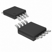
LTC1877EMS8#TR Linear Technology, LTC1877EMS8#TR Datasheet - Page 7

LTC1877EMS8#TR
Manufacturer Part Number
LTC1877EMS8#TR
Description
IC BUCK SYNC ADJ .6A 8MSOP
Manufacturer
Linear Technology
Type
Step-Down (Buck)r
Datasheet
1.LTC1877EMS8PBF.pdf
(16 pages)
Specifications of LTC1877EMS8#TR
Internal Switch(s)
Yes
Synchronous Rectifier
Yes
Number Of Outputs
1
Voltage - Output
0.8 ~ 10 V
Current - Output
600mA
Frequency - Switching
550kHz
Voltage - Input
2.65 ~ 10 V
Operating Temperature
-40°C ~ 85°C
Mounting Type
Surface Mount
Package / Case
8-MSOP, Micro8™, 8-uMAX, 8-uSOP,
Lead Free Status / RoHS Status
Contains lead / RoHS non-compliant
Power - Output
-
Available stocks
Company
Part Number
Manufacturer
Quantity
Price
OPERATION
The LTC1877 uses a constant-frequency, current mode
step-down architecture. Both the main (P-channel MOS-
FET) and synchronous (N-channel MOSFET) switches are
internal. During normal operation, the internal top power
MOSFET is turned on each cycle when the oscillator sets
the RS latch, and turned off when the current comparator,
I
which I
age on the I
EA. The V
allows EA to receive an output feedback voltage from an
external resistive divider. When the load current increases,
it causes a slight decrease in the feedback voltage relative
to the 0.8V reference, which in turn, causes the I
to increase until the average inductor current matches the
new load current. While the top MOSFET is off, the bottom
MOSFET is turned on until either the inductor current starts
to reverse as indicated by the current reversal comparator
I
Comparator OVDET guards against transient overshoots
> 6.25% by turning the main switch off and keeping it off
until the fault is removed.
Burst Mode Operation
The LTC1877 is capable of Burst Mode operation in which
the internal power MOSFETs operate intermittently based
on load demand. To enable Burst Mode operation, simply
tie the SYNC/MODE pin to V
high (V
tion and enable PWM pulse-skipping mode, connect the
SYNC/MODE pin to GND. In this mode, the effi ciency is
lower at light loads, but becomes comparable to Burst
Mode operation when the output load exceeds 50mA. The
advantage of pulse-skipping mode is lower output ripple
and less interference to audio circuitry.
When the converter is in Burst Mode operation, the peak
current of the inductor is set to approximately 250mA,
even though the voltage at the I
value. The voltage at the I
average current is greater than the load requirement. As the
I
comparator trips, causing the internal sleep line to go
high and forces off both power MOSFETs. The I
COMP
RCMP
TH
voltage drops below approximately 0.55V, the BURST
, resets the RS latch. The peak inductor current at
, or the beginning of the next clock cycle.
COMP
SYNC/MODE
FB
TH
pin, described in the Pin Functions section,
resets the RS latch is controlled by the volt-
pin, which is the output of error amplifi er
> 1.5V). To disable Burst Mode opera-
(Refer to Functional Diagram)
TH
pin drops when the inductor’s
IN
TH
or connect it to a logic
pin indicates a lower
TH
TH
voltage
pin is
then disconnected from the output of the EA amplifi er and
parked a diode voltage above ground.
In sleep mode, both power MOSFETs are held off and a
majority of the internal circuitry is partially turned off,
reducing the quiescent current to 10μA. The load current
is now being supplied solely from the output capacitor.
When the output voltage drops, the I
to the output of the EA amplifi er and the top MOSFET is
again turned on and this process repeats.
Short-Circuit Protection
When the output is shorted to ground, the frequency of
the oscillator is reduced to about 80kHz, one-seventh the
nominal frequency. This frequency foldback ensures that
the inductor current has ample time to decay, thereby
preventing runaway. The oscillator’s frequency will progres-
sively increase to 550kHz (or the synchronized frequency)
when V
Frequency Synchronization
A phase-locked loop (PLL) is available on the LTC1877 to
allow the internal oscillator to be synchronized to an external
source connected to the SYNC/MODE pin. The output of
the phase detector at the PLL LPF pin operates over a 0V
to 2.4V range corresponding to 400kHz to 700kHz. When
locked, the PLL aligns the turn-on of the top MOSFET to
the rising edge of the synchronizing signal.
When the LTC1877 is clocked by an external source, Burst
Mode operation is disabled; the LTC1877 then operates in
PWM pulse-skipping mode. In this mode, when the output
load is very low, current comparator I
tripped for several cycles and force the main switch to stay
off for the same number of cycles. Increasing the output
load slightly allows constant-frequency PWM operation
to resume. This mode exhibits low output ripple as well
as low audio noise and reduced RF interference while
providing reasonable low current effi ciency.
Frequency synchronization is inhibited when the feedback
voltage V
from interfering with the frequency foldback for short-
circuit protection.
FB
FB
rises above 0.3V.
is below 0.6V. This prevents the external clock
TH
COMP
LTC1877
pin reconnects
may remain
1877fa
7


