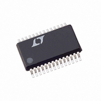
LTC3703EG-5#TR Linear Technology, LTC3703EG-5#TR Datasheet - Page 18

LTC3703EG-5#TR
Manufacturer Part Number
LTC3703EG-5#TR
Description
IC BUCK/BOOST SYNC ADJ 5A 28SSOP
Manufacturer
Linear Technology
Type
Step-Down (Buck), Step-Up (Boost)r
Datasheet
1.LTC3703EGN-5PBF.pdf
(32 pages)
Specifications of LTC3703EG-5#TR
Internal Switch(s)
No
Synchronous Rectifier
Yes
Number Of Outputs
1
Voltage - Output
0.8 ~ 55.8 V
Current - Output
5A
Frequency - Switching
100kHz ~ 600kHz
Voltage - Input
9.3 ~ 60 V
Operating Temperature
-40°C ~ 85°C
Mounting Type
Surface Mount
Package / Case
28-SSOP
Lead Free Status / RoHS Status
Contains lead / RoHS non-compliant
Power - Output
-
LTC3703-5
APPLICATIO S I FOR ATIO
node dV/dt can be many volts/ns, which will pull up on the
gate of the bottom MOSFET through its Miller capacitance.
If this Miller current, times the internal gate resistance of
the MOSFET plus the driver resistance, exceeds the thresh-
old of the FET, shoot-through will occur. By using a nega-
tive supply on BGRTN, the BG can be pulled below ground
when turning the bottom MOSFET off. This provides a few
extra volts of margin before the gate reaches the turn-on
threshold of the MOSFET. Be aware that the maximum
voltage difference between DRV
for example, V
DRV
Current Limit Programming
Programming current limit on the LTC3703-5 is straight
forward. The I
maximum allowable voltage drop across the bottom
MOSFET. The voltage across the MOSFET is set by its on-
resistance and the current flowing in the inductor, which
is the same as the output current. The LTC3703-5 current
limit circuit inverts the negative voltage across the MOSFET
before comparing it to the voltage at I
current limit to be set with a positive voltage.
To set the current limit, calculate the expected voltage
drop across the bottom MOSFET at the maximum desired
current and maximum junction temperature:
where δ is explained in the MOSFET Selection section.
V
internal 12µA pull-up and an external resistor:
The current limit value should be checked to ensure that
I
generally occurs with the largest V
ent temperature, conditions that cause the largest power
loss in the converter. Note that it is important to check for
self-consistency between the assumed MOSFET junction
temperature and the resulting value of I
the MOSFET switches.
Caution should be used when setting the current limit
based upon the R
current limit is determined by the minimum MOSFET on-
18
LIMIT(MIN)
PROG
V
R
PROG
IMAX
CC
is then programmed at the I
pin is now 13V instead of 15V.
= V
= (I
> I
PROG
OUT(MAX)
LIMIT
MAX
BGRTN
/12µA
DS(ON)
)(R
pin sets the current limit by setting the
U
DS(ON)
. The minimum value of current limit
= –2V, the maximum voltage on
of the MOSFETs. The maximum
U
)(1 + δ)
CC
IN
and BGRTN is 15V. If,
W
at the highest ambi-
MAX
MAX
LIMIT
pin using the
, allowing the
which heats
U
resistance. Data sheets typically specify nominal and
maximum values for R
reasonable assumption is that the minimum R
the same amount below the typical value as the maximum
lies above it. Consult the MOSFET manufacturer for further
guidelines.
For best results, use a V
500mV. Values outside of this range may give less accu-
rate current limit. The current limit can also be disabled by
floating the I
FEEDBACK LOOP/COMPENSATION
Feedback Loop Types
In a typical LTC3703-5 circuit, the feedback loop consists
of the modulator, the external inductor, the output capaci-
tor and the feedback amplifier with its compensation
network. All of these components affect loop behavior and
must be accounted for in the loop compensation. The
modulator consists of the internal PWM generator, the
output MOSFET drivers and the external MOSFETs them-
selves. From a feedback loop point of view, it looks like a
linear voltage transfer function from COMP to SW and has
a gain roughly equal to the input voltage. It has fairly
benign AC behavior at typical loop compensation frequen-
cies with significant phase shift appearing at half the
switching frequency.
The external inductor/output capacitor combination makes
a more significant contribution to loop behavior. These
components cause a second order LC roll off at the output,
with the attendant 180° phase shift. This rolloff is what filters
the PWM waveform, resulting in the desired DC output
voltage, but the phase shift complicates the loop compen-
sation if the gain is still higher than unity at the pole fre-
quency. Eventually (usually well above the LC pole
frequency), the reactance of the output capacitor will ap-
proach its ESR and the rolloff due to the capacitor will stop,
leaving 6dB/octave and 90° of phase shift (Figure 10).
So far, the AC response of the loop is pretty well out of the
user’s control. The modulator is a fundamental piece of the
LTC3703-5 design and the external L and C are usually
chosen based on the regulation and load current require-
ments without considering the AC loop response. The
MAX
pin.
PROG
DS(ON)
voltage between 100mV and
, but not a minimum. A
DS(ON)
37035fa
lies


