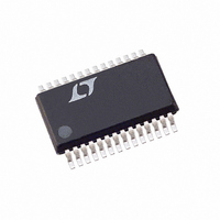
LTC3703EG-5#TR Linear Technology, LTC3703EG-5#TR Datasheet - Page 3

LTC3703EG-5#TR
Manufacturer Part Number
LTC3703EG-5#TR
Description
IC BUCK/BOOST SYNC ADJ 5A 28SSOP
Manufacturer
Linear Technology
Type
Step-Down (Buck), Step-Up (Boost)r
Datasheet
1.LTC3703EGN-5PBF.pdf
(32 pages)
Specifications of LTC3703EG-5#TR
Internal Switch(s)
No
Synchronous Rectifier
Yes
Number Of Outputs
1
Voltage - Output
0.8 ~ 55.8 V
Current - Output
5A
Frequency - Switching
100kHz ~ 600kHz
Voltage - Input
9.3 ~ 60 V
Operating Temperature
-40°C ~ 85°C
Mounting Type
Surface Mount
Package / Case
28-SSOP
Lead Free Status / RoHS Status
Contains lead / RoHS non-compliant
Power - Output
-
Note 1: Absolute Maximum Ratings are those values beyond which the life
of a device may be impaired.
Note 2: The LTC3703-5 is guaranteed to meet performance specifications
from 0°C to 70°C. Specifications over the –40°C to 85°C operating
temperature range are assured by design, characterization and correlation
with statistical process controls. The LTC3703I-5 is guaranteed over the full
–40°C to 125°C operating junction temperature range.
Note 3: T
dissipation P
Note 4: The LTC3703-5 is tested in a feedback loop that servos V
SYMBOL
Main Control Loop
V
∆V
∆V
V
∆V
I
V
I
I
I
V
V
I
V
Oscillator
f
f
t
DC
Driver
I
R
I
R
Feedback Amplifier
A
f
I
I
ELECTRICAL CHARACTERISTICS
temperature range, otherwise specifications are at T
BGRTN = 0V, RUN/SS = I
MODE/SYNC
INV
VIN
MAX
RUN/SS
OSC
SYNC
ON, MIN
BG, PEAK
TG, PEAK
U
FB
COMP
FB
MODE/SYNC
INV
OS, IMAX
RUN/SS
UV
VOL
BG, SINK
TG, SINK
FB, LINE
FB, LOAD
MODE/SYNC
MAX
LTC3703-5: T
J
is calculated from the ambient temperature T
D
according to the following formula:
J
= T
PARAMETER
Feedback Voltage
Feedback Voltage Line Regulation
Feedback Voltage Load Regulation
MODE/SYNC Threshold
MODE/SYNC Hysteresis
MODE/SYNC Current
Invert Threshold
Invert Current
V
I
V
Shutdown Threshold
RUN/SS Source Current
Maximum RUN/SS Sink Current
Undervoltage Lockout
Oscillator Frequency
External Sync Frequency Range
Minimum On-Time
Maximum Duty Cycle
BG Driver Peak Source Current
BG Driver Pull-Down R
TG Driver Peak Source Current
TG Driver Pull-Down R
Op Amp DC Open Loop Gain
Op Amp Unity Gain Crossover Frequency (Note 6)
FB Input Current
COMP Sink/Source Current
A
MAX
IN
IMAX
+ (P
Sense Input Current
Source Current
D
Offset Voltage
MAX
• 100 °C/W) G Package
= open, R
DS, ON
SET
DS, ON
= 25k, unless otherwise specified.
A
and power
A
= 25°C. V
FB
CONDITIONS
(Note 4)
5V < V
1V < V
MODE/SYNC Rising
0 ≤ V
0 ≤ V
V
RUN/SS = 0V, V
V
|V
RUN/SS = 0V
|V
V
V
Hysteresis
R
f < 200kHz
(Note 8)
(Note 8)
(Note 4)
0 ≤ V
IN
IMAX
CC
CC
SET
SW
SW
to the
The
= 60V
Rising
Falling
| – V
| – V
MODE/SYNC
INV
= 25kΩ
FB
= 0V
CC
COMP
●
≤ 3V
CC
≤ 15V
< 15V (Note 4)
IMAX
IMAX
denotes the specifications which apply over the full operating
= DRV
< 2V (Note 4)
at I
> 100mV
reference voltage with the COMP pin forced to a voltage between 1V and 2V.
Note 5: The dynamic input supply current is higher due to the power
MOSFET gate charging being delivered at the switching frequency
(Q
Note 6: Guaranteed by design. Not subject to test.
Note 7: This IC includes overtemperature protection that is intended to
protect the device during momentary overload conditions. Junction
temperature will exceed 125°C when overtemperature protection is active.
Continuous operation above the specified maximum operating junction
temperature may impair device reliability.
Note 8: R
IN
≤ 15V
G
RUN/SS
= 10V
CC
• f
OSC
= V
DS(ON)
).
= 0µA
BOOST
guaranteed by correlation to wafer level measurement.
= V
IN
= 5V, V
●
●
●
●
●
●
MODE/SYNC
0.792
0.788
10.5
0.45
0.75
0.75
MIN
– 25
0.75
270
100
2.3
3.4
2.8
0.7
89
74
±5
9
1
= V
LTC3703-5
0.800
0.007
0.01
0.65
TYP
300
200
±10
INV
0.8
1.5
0.9
3.8
3.7
3.1
1.2
1.2
10
20
80
17
93
85
25
12
0
0
1
1
0
0
= V
SW
0.808
0.812
MAX
0.05
0.87
13.5
0.85
130
330
600
0.1
1.2
5.3
4.1
3.4
1.8
1.8
55
25
96
=
1
2
1
1
1
UNITS
37035fa
3
MHz
%/V
kHz
kHz
mV
mV
mA
µA
µA
µA
µA
µA
µA
µA
dB
µA
ns
%
%
Ω
Ω
V
V
V
V
V
V
V
V
A
A


