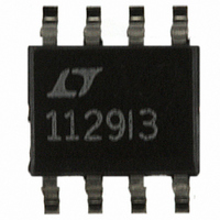
LT1107CS8 Linear Technology, LT1107CS8 Datasheet - Page 10

LT1107CS8
Manufacturer Part Number
LT1107CS8
Description
IC DC/DC CONV ADJUSTBL OUT 8SOIC
Manufacturer
Linear Technology
Type
Step-Down (Buck), Step-Up (Boost), Invertingr
Datasheet
1.LT1107CS8PBF.pdf
(16 pages)
Specifications of LT1107CS8
Internal Switch(s)
Yes
Synchronous Rectifier
No
Number Of Outputs
1
Voltage - Output
Adjustable
Current - Output
400mA
Frequency - Switching
63kHz
Voltage - Input
2 ~ 30 V
Operating Temperature
0°C ~ 70°C
Mounting Type
Surface Mount
Package / Case
8-SOIC (3.9mm Width)
Power - Output
500mW
Lead Free Status / RoHS Status
Contains lead / RoHS non-compliant
Available stocks
Company
Part Number
Manufacturer
Quantity
Price
Company:
Part Number:
LT1107CS8
Manufacturer:
LT
Quantity:
5 510
Part Number:
LT1107CS8
Manufacturer:
LINEAR/凌特
Quantity:
20 000
Part Number:
LT1107CS8#PBF
Manufacturer:
LINEAR/凌特
Quantity:
20 000
Part Number:
LT1107CS8#TRPBF
Manufacturer:
LINEAR/凌特
Quantity:
20 000
Part Number:
LT1107CS8-12
Manufacturer:
LINEAR/凌特
Quantity:
20 000
Part Number:
LT1107CS8-12#PBF
Manufacturer:
LINEAR/凌特
Quantity:
20 000
LT1107
voltages can be accommodated as in the prior section.
In Figure 4, the input is negative while the output is
positive. In this configuration, the magnitude of the input
voltage can be higher or lower than the output voltage. A
level shift, provided by the PNP transistor, supplies proper
polarity feedback information to the regulator.
A
10
–V
V
+V
PPLICATI
IN
OUT
IN
+
+
should be less than 6.2V. More negative output
C2
C2
Figure 3. Positive-to-Negative Converter
Figure 4. Negative-to-Positive Converter
I
LIM
I
GND
LIM
R3
R3
O
LT1107
LT1107
GND
V
IN
U
SW2
V
S
IN
SW1
SW1
SW2
FB
FB
I FOR ATIO
L1
U
D1
1N5818
R2
L1
D1
W
V
OUT
+
+
=
C1
R1
R2
C1
1.25V + 0.6V
U
2N3906
R2
R1
R1
+V
–V
1107 F04
1107 F03
OUT
OUT
Using the I
The LT1107 switch can be programmed to turn off at a set
switch current, a feature not found on competing devices.
This enables the input to vary over a wide range without
exceeding the maximum switch rating or saturating the
inductor. Consider the case where analysis shows the
LT1107 must operate at an 800mA peak switch current
with a 2V input. If V
will rise to 1.6A, exceeding the maximum switch current
rating. With the proper resistor selected (see the “Maxi-
mum Switch Current vs R
current will be limited to 800mA, even if the input voltage
increases.
Another situation where the I
when the device goes into continuous mode operation.
This occurs in step-up mode when:
When the input and output voltages satisfy this relation-
ship, inductor current does not go to zero during the
switch OFF time. When the switch turns on again, the
current ramp starts from the non-zero current level in the
inductor just prior to switch turn-on. As shown in Figure
5, the inductor current increases to a high level before the
comparator turns off the oscillator. This high current can
cause excessive output ripple and requires oversizing the
output capacitor and inductor. With the I
switch turns off at the programmed current as shown in
Figure 6, keeping output ripple to a minimum.
V
OUT
V
IN
LIM
V
V
DIODE
SW
Pin
IN
1
rises to 4V, the peak switch current
1
DC
LIM
” characteristic), the switch
LIM
feature is useful occurs
LIM
feature, the
1107fa
( )
24


