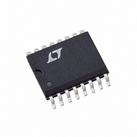
LTC1149CS-5 Linear Technology, LTC1149CS-5 Datasheet - Page 13

LTC1149CS-5
Manufacturer Part Number
LTC1149CS-5
Description
IC SW REG STEP-DOWN 5V 16-SOIC
Manufacturer
Linear Technology
Type
Step-Down (Buck)r
Datasheet
1.LTC1149CNPBF.pdf
(20 pages)
Specifications of LTC1149CS-5
Internal Switch(s)
No
Synchronous Rectifier
Yes
Number Of Outputs
1
Voltage - Output
5V
Current - Output
50mA
Frequency - Switching
250kHz
Voltage - Input
0 ~ 48 V
Operating Temperature
0°C ~ 70°C
Mounting Type
Surface Mount
Package / Case
16-SOIC (3.9mm Width)
Lead Free Status / RoHS Status
Contains lead / RoHS non-compliant
Power - Output
-
Available stocks
Company
Part Number
Manufacturer
Quantity
Price
Part Number:
LTC1149CS-5
Manufacturer:
LINEAR/凌特
Quantity:
20 000
Part Number:
LTC1149CS-5#TRPBF
Manufacturer:
LINEAR/凌特
Quantity:
20 000
APPLICATIO S I FOR ATIO
LTC1149 Package Dissipation
High input voltage applications in which large MOSFETs
are being driven at high frequencies may cause the maxi-
mum junction temperature rating for the LTC1149 series
to be exceeded. The LTC1149 supply current is dominated
by the gate charge supply current, which is given as a
function of operating frequency in the Typical Perfor-
mance Characteristics. The LTC1149 series junction tem-
perature can be estimated by using the equations given in
Note 1 of the Electrical Characteristics. For example, the
LT1149CS is limited to less than 11mA from a 48V supply:
To prevent the maximum junction temperature from being
exceeded, the Pin 2 supply current must be checked in
continuous mode when operating at the maximum V
Design Example
As a design example, assume V
I
immediately be calculated:
Selection of the P-channel MOSFET involves doing calcu-
lations for different sized MOSFETs to determine the
relative loss contributions. Taking an International Recti-
fier IRF9Z34 for example, R
Q
can be used to estimate the I
and gate charge supply current losses:
MAX
P
T
R
C
L
Est. I
(5V/24V)(2.5)
Est. Transition Loss =
5(24V)
Est. Gate Charge Loss =
(100kHz)(35nC)(24V) = 85mW
= 35nC and C
J
MIN
T
SENSE
= 70 C + (11mA)(48V)(110 C/W)
= 128 C exceeds absolute maximum
= 2.5A and f = 100kHz. R
=
(7.8)(10
2
= (5.1)(10
R Loss (T
2
100kHz
(2.5A)(200pF)(100kHz) = 145mW
= 100mV
2.5
RSS
–5
2
(1 + 0.5)0.14 = 270mW
J
)
5
U U
= 100 C) =
)(0.039 )(620pF)(5V) = 62 H
= 200pF (V
1 –
= 0.039
24V
5V
2
R losses, transition losses
DS
= 620pF
DS(ON)
IN
SENSE
= V
W
= 24V, V
IN
/2). These values
, C
= 0.14
T
and L can
OUT
U
= 5V,
Max,
IN
.
The same calculations were repeated for a smaller device,
the Motorola MTD2955 (R
the Harris RFP30P05 (R
summarized in the table.
For this set of conditions, the midsized P-channel MOSFET
actually produces the lowest total losses at I
resulting efficiency differences will be even more pro-
nounced at lower output currents. Note that only the I
and transition losses are dissipated in the MOSFET; the
gate charge supply current loss is dissipated by the
LTC1149 series.
Selection of the N-channel MOSFET is somewhat easier; it
need only be sized for the anticipated I
duty cycle (worst-case assumption for short circuit.) The
Siliconix Si9410, for example, has R
and Q
100 C and a gate charge supply current loss of 75mW. As
with the P-channel device, the use of a larger MOSFET may
actually result in lower midcurrent efficiency.
C
temperature, and C
optimum efficiency. The output capacitor ESR require-
ment can be fulfilled by a single OS-CON or by two or more
surface mount tantalums in parallel.
Auxiliary Windings – Suppressing Burst Mode
Operation
The LTC1149 synchronous switch removes the normal
limitation that power must be drawn from the inductor
primary winding in order to extract power from auxiliary
windings. With synchronous switching, auxiliary outputs
may be loaded without regard to the primary output load,
providing that the loop remains in continuous mode
operation.
Burst Mode operation can be suppressed at low output
currents with a simple external network which cancels the
IN
Est. I
Est. Transition Loss
Est. Gate Charge Loss
Est. Total Loss
F = 100kHz, I
V
will require an RMS current rating of at least 1.25A at
IN
2
CONDITIONS
= 24V, V
N
R Loss (100 C)
= 30nC. This will produce an I
OUT
OUT
= 2.5A
= 5V
LTC1149-3.3/LTC1149-5
OUT
will require an ESR of 0.04 for
DS(ON)
MTD2955
550mW
110mW
720mW
60mW
DS(ON)
= 0.065 ). The results are
P-CHANNEL MOSFET
= 0.3 ) and a larger one,
IRF9Z34
270mW
145mW
500mW
DS(ON)
2
85mW
R loss of 250mW at
2
R losses at 100%
LTC1149
= 0.03 Max
RFP30P05
MAX
120mW
290mW
240mW
650mW
13
. The
2
R


