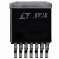
LT1374CR-5 Linear Technology, LT1374CR-5 Datasheet - Page 14

LT1374CR-5
Manufacturer Part Number
LT1374CR-5
Description
IC SW REG 4.5A 5V STEP-DWN 7-DD
Manufacturer
Linear Technology
Type
Step-Down (Buck)r
Datasheet
1.LT1374CFEPBF.pdf
(32 pages)
Specifications of LT1374CR-5
Internal Switch(s)
Yes
Synchronous Rectifier
No
Number Of Outputs
1
Voltage - Output
5V
Current - Output
4.5A
Frequency - Switching
500kHz
Voltage - Input
5 ~ 25 V
Operating Temperature
0°C ~ 125°C
Mounting Type
Surface Mount
Package / Case
D²Pak, TO-263 (7 leads + tab)
Lead Free Status / RoHS Status
Contains lead / RoHS non-compliant
Power - Output
-
Available stocks
Company
Part Number
Manufacturer
Quantity
Price
Company:
Part Number:
LT1374CR-5
Manufacturer:
Linear Technology
Quantity:
135
Company:
Part Number:
LT1374CR-5
Manufacturer:
DSP
Quantity:
2 000
Company:
Part Number:
LT1374CR-5#PBF
Manufacturer:
LT
Quantity:
1 900
Part Number:
LT1374CR-5#PBF
Manufacturer:
LINEAR/凌特
Quantity:
20 000
Company:
Part Number:
LT1374CR-5#TRPBF
Manufacturer:
LT
Quantity:
1 900
Company:
Part Number:
LT1374CR-5.0
Manufacturer:
LT
Quantity:
1
LT1374
APPLICATIONS
that it can be recharged fully under the worst-case condi-
tion of minimum input voltage. Almost any type of film or
ceramic capacitor will work fine.
WARNING! Peak voltage on the BOOST pin is the sum of
unregulated input voltage plus the voltage across the
boost capacitor. This normally means that peak BOOST
pin voltage is equal to input voltage plus output voltage,
but when the boost diode is connected to the regulator
input, peak BOOST pin voltage is equal to twice the input
voltage. Be sure that BOOST pin voltage does not exceed
its maximum rating .
For nearly all applications, a 0.27µF boost capacitor works
just fine, but for the curious, more details are provided
here. The size of the boost capacitor is determined by
switch drive current requirements. During switch on time,
drain current on the capacitor is approximately I
peak load current of 4.25A, this gives a total drain of 85mA.
Capacitor ripple voltage is equal to the product of on time
and drain current divided by capacitor value;
∆V = (t
less than 0.6V (a slightly arbitrary number) at the worst-
case condition of t
0.27µF. Boost capacitor ripple voltage is not a critical
parameter, but if the minimum voltage across the capaci-
tor drops to less than 3V, the power switch may not
saturate fully and efficiency will drop. An approximate
formula for absolute minimum capacitor value is:
14
ON
)(85mA/C). To keep capacitor ripple voltage to
INPUT
ON
U
C1
= 1.8µs, the capacitor needs to be
INFORMATION
U
R
R
LO
HI
IN
SHDN
W
LT1374
Figure 4. Undervoltage Lockout
3.5µA
OUT
U
/ 50. At
2.38V
0.4V
GND
R
FB
+
–
+
–
f = Switching frequency
V
V
This formula can yield capacitor values substantially less
than 0.27µF, but it should be used with caution since it
does not take into account secondary factors such as
capacitor series resistance, capacitance shift with tem-
perature and output overload.
SHUTDOWN FUNCTION AND
UNDERVOLTAGE LOCKOUT
Figure 4 shows how to add undervoltage lockout (UVLO)
to the LT1374. Typically, UVLO is used in situations where
the input supply is current limited , or has a relatively high
source resistance. A switching regulator draws constant
power from the source, so source current increases as
source voltage drops. This looks like a negative resistance
load to the source and can cause the source to current limit
or latch low under low source voltage conditions. UVLO
prevents the regulator from operating at source voltages
where these problems might occur.
OUT
IN
= Minimum input voltage
= Regulated output voltage
STANDBY
TOTAL
SHUTDOWN
V
SW
+
OUTPUT
1374 F04
1374fd


