LT1374CR-5 Linear Technology, LT1374CR-5 Datasheet - Page 3
LT1374CR-5
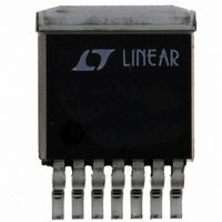
Manufacturer Part Number
LT1374CR-5
Description
IC SW REG 4.5A 5V STEP-DWN 7-DD
Manufacturer
Linear Technology
Type
Step-Down (Buck)r
Datasheet
1.LT1374CFEPBF.pdf
(32 pages)
Specifications of LT1374CR-5
Internal Switch(s)
Yes
Synchronous Rectifier
No
Number Of Outputs
1
Voltage - Output
5V
Current - Output
4.5A
Frequency - Switching
500kHz
Voltage - Input
5 ~ 25 V
Operating Temperature
0°C ~ 125°C
Mounting Type
Surface Mount
Package / Case
D²Pak, TO-263 (7 leads + tab)
Lead Free Status / RoHS Status
Contains lead / RoHS non-compliant
Power - Output
-
Available stocks
Company
Part Number
Manufacturer
Quantity
Price
Company:

Part Number:
LT1374CR-5
Manufacturer:
Linear Technology
Quantity:
135
Company:
Part Number:
LT1374CR-5
Manufacturer:
DSP
Quantity:
2 000
Company:
Part Number:
LT1374CR-5#PBF
Manufacturer:
LT
Quantity:
1 900
Part Number:
LT1374CR-5#PBF
Manufacturer:
LINEAR/凌特
Quantity:
20 000
Company:
Part Number:
LT1374CR-5#TRPBF
Manufacturer:
LT
Quantity:
1 900
Company:
Part Number:
LT1374CR-5.0
Manufacturer:
LT
Quantity:
1


ELECTRICAL CHARACTERISTICS
Note 1: Absolute Maximum Ratings are those values beyond which the life
of a device may be impaired.
Note 2: Gain is measured with a V
switching threshold level to 200mV below the upper clamp level.
Note 3: Minimum input voltage is not measured directly, but is guaranteed
by other tests. It is defined as the voltage where internal bias lines are still
ture range, otherwise specifications are at T
PARAMETER
Feedback Voltage (Adjustable)
Sense Voltage (Fixed 5V)
SENSE Pin Resistance
Reference Voltage Line Regulation
Feedback Input Bias Current
Error Amplifier Voltage Gain
Error Amplifier Transconductance
V
Error Amplifier Source Current
Error Amplifier Sink Current
V
V
Switch Current Limit
Slope Compensation (Note 9)
Switch On Resistance (Note 7)
Maximum Switch Duty Cycle
Switch Frequency
Switch Frequency Line Regulation
Frequency Shifting Threshold on FB Pin
Minimum Input Voltage (Note 3)
Minimum Boost Voltage (Note 4)
Boost Current (Note 5)
V
BIAS Supply Current (Note 6)
Shutdown Supply Current
Lockout Threshold
Shutdown Thresholds
Synchronization Threshold
Synchronizing Range
SYNC Pin Input Resistance
C
C
C
IN
Pin to Switch Current Transconductance
Pin Switching Threshold
Pin High Clamp
Supply Current (Note 6)
C
swing equal to 200mV above the
CONDITIONS
All Conditions
All Conditions
5V ≤ V
(Notes 2, 8)
∆I (V
V
V
Duty Cycle = 0
V
DC = 80%
I
V
V
5V ≤ V
∆f = 10kHz
I
I
I
V
V
V
V
V
V
Device Starting Up
SW
SW
SW
SW
FB
FB
C
FB
C
BIAS
BIAS
SHDN
SHDN
C
C
Open, V
Set to Give 50% Duty Cycle
Open
Open Device Shutting Down
J
= 2.1V or V
= 2.7V or V
= 4.5A
= 2.1V or V
≤ 4.5A
= 1A
= 4.5A
C
= 25°C. V
= 5V
= 5V
) = ±10µA (Note 8)
IN
IN
= 0V, V
= 0V, V
≤ 25V, (5V ≤ V
≤ 25V (5V ≤ V
FB
= 2.1V or V
IN
IN
SENSE
SENSE
SENSE
IN
≤ 25V, V
≤ 32V, V
= 15V, V
The
= 4.4V
= 5.6V
= 4.4V
IN
IN
●
SENSE
SW
SW
≤ 32V for LT1374HV)
≤ 32V for LT1374HV)
denotes specifications which apply over the full operating tempera-
= 0V, V
= 0V, V
C
= 1.5V, Boost = V
= 4.4V, DC ≤ 50%
regulated so that the reference voltage and oscillator frequency remain
constant. Actual minimum input voltage to maintain a regulated output will
depend on output voltage and load current. See Applications Information.
Note 4: This is the minimum voltage across the boost capacitor needed to
guarantee full saturation of the internal power switch.
C
C
Open
Open
IN
+ 5V, switch open, unless otherwise noted.
●
●
●
●
●
●
●
●
●
●
●
●
●
●
●
●
●
●
●
●
●
●
●
●
1500
1000
MIN
2.39
2.36
4.94
4.90
0.13
0.25
200
140
140
460
440
580
4.5
0.8
2.3
90
86
7
2000
2.42
0.01
0.07
2.38
0.37
0.45
TYP
400
225
225
500
5.0
0.5
5.3
0.9
2.1
0.8
1.0
5.0
2.3
0.9
3.2
1.5
10
93
93
20
90
20
30
40
6
0
2700
3100
1000
MAX
2.45
2.48
5.06
5.10
0.03
0.13
0.15
2.46
0.60
320
320
540
560
140
100
8.5
0.1
1.3
5.5
3.0
1.4
4.0
0.7
2.2
14
35
50
75
75
2
LT1374
UNITS
µMho
µMho
1374fd
3
%/ V
%/V
A/ V
kHz
kHz
kHz
mA
mA
mA
mA
kΩ
kΩ
µA
µA
µA
µA
µA
µA
µA
%
%
Ω
Ω
V
V
V
V
V
V
A
A
V
V
V
V
V
V
V
Related parts for LT1374CR-5
Image
Part Number
Description
Manufacturer
Datasheet
Request
R

Part Number:
Description:
4.5A/ 500kHz Step-Down Switching Regulator
Manufacturer:
Linear Technology
Datasheet:

Part Number:
Description:
4.5A, 500kHz Step-Down Switching Regulator
Manufacturer:
Linear Technology Corporation
Datasheet:
Part Number:
Description:
CD ROM LINEARVIEW DATASHEETS
Manufacturer:
Linear Technology
Part Number:
Description:
Standalone Linear Li-Ion Battery Charger with Thermal Regulation in ThinSOT
Manufacturer:
Linear Technology Corporation
Datasheet:
Part Number:
Description:
Low noise, high frequency, 8th order linear phase lowpass filter
Manufacturer:
Linear Technology Corporation
Datasheet:
Part Number:
Description:
Manufacturer:
Linear Technology Corporation
Datasheet:
Part Number:
Description:
Manufacturer:
Linear Technology Corporation
Datasheet:
Part Number:
Description:
Manufacturer:
Linear Technology Corporation
Datasheet:
Part Number:
Description:
Manufacturer:
Linear Technology Corporation
Datasheet:
Part Number:
Description:
Manufacturer:
Linear Technology Corporation
Datasheet:
Part Number:
Description:
Manufacturer:
Linear Technology Corporation
Datasheet:
Part Number:
Description:
Manufacturer:
Linear Technology Corporation
Datasheet:
Part Number:
Description:
Dual and Quad, JFET Input Precision High Speed Op Amps
Manufacturer:
Linear Technology Corporation
Datasheet:
Part Number:
Description:
Manufacturer:
Linear Technology Corporation
Datasheet:
Part Number:
Description:
1, 2, 6 and 8 Channel, 10-Bit Serial I/O Data Acquisition Systems
Manufacturer:
Linear Technology Corporation
Datasheet: