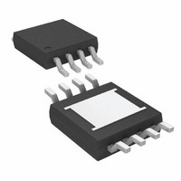
LT3505EMS8E#PBF Linear Technology, LT3505EMS8E#PBF Datasheet - Page 7

LT3505EMS8E#PBF
Manufacturer Part Number
LT3505EMS8E#PBF
Description
IC REG SW STP DWN 1.2A 8-MSOP
Manufacturer
Linear Technology
Type
Step-Down (Buck)r
Datasheet
1.LT3505EDDPBF.pdf
(24 pages)
Specifications of LT3505EMS8E#PBF
Internal Switch(s)
Yes
Synchronous Rectifier
No
Number Of Outputs
1
Voltage - Output
0.78 ~ 33.8 V
Current - Output
1.2A
Frequency - Switching
200kHz ~ 3MHz
Voltage - Input
3.6 ~ 36 V
Operating Temperature
-40°C ~ 85°C
Mounting Type
Surface Mount
Package / Case
8-MSOP Exposed Pad, 8-HMSOP, 8-eMSOP
Dc To Dc Converter Type
Step Down
Pin Count
8
Input Voltage
36V
Output Voltage
0.78 to 33.84V
Switching Freq
200 TO 3000KHz
Output Current
1.2A
Package Type
MSOP EP
Output Type
Adjustable
Switching Regulator
Yes
Line Regulation
0.007%/V(Typ)
Mounting
Surface Mount
Input Voltage (min)
3.6V
Operating Temp Range
-40C to 85C
Operating Temperature Classification
Industrial
Lead Free Status / RoHS Status
Lead free / RoHS Compliant
Power - Output
-
Lead Free Status / Rohs Status
Compliant
Available stocks
Company
Part Number
Manufacturer
Quantity
Price
PIN FUNCTIONS
BOOST (Pin 1): The BOOST pin is used to provide a drive
voltage, higher than the input voltage, to the internal bipolar
NPN power switch.
SW (Pin 2): The SW pin is the output of the internal power
switch. Connect this pin to the inductor, catch diode and
boost capacitor.
V
internal regulator and to the internal power switch. This
pin must be locally bypassed.
SHDN (Pin 4): The SHDN pin is used to put the LT3505 in
shutdown mode. Tie to ground to shut down the LT3505.
Tie to 2.3V or more for normal operation. If the shutdown
feature is not used, tie this pin to the V
provides a soft-start function; see the Applications Infor-
mation section.
GND (Pin 5): Tie the GND pin to a local ground plane
below the LT3505 and the circuit components. Return the
feedback divider to this pin.
IN
(Pin 3): The V
IN
pin supplies current to the LT3505’s
IN
pin. SHDN also
R
frequency of the LT3505 by connecting a resistor from
this pin to ground. The Applications Information section of
the data sheet includes a table to determine the resistance
value based on the desired switching frequency. Minimize
capacitance at this pin.
FB (Pin 7): The LT3505 regulates its feedback pin to 780mV.
Connect the feedback resistor divider tap to this pin. Set
the output voltage by selecting R1 according to:
A good value for R2 is 10.0k.
V
control loop by tying an external RC network from this
pin to ground.
Exposed Pad (Pin 9): The Exposed Pad must be soldered
to the PCB and electrically connected to ground. Use a
large ground plane and thermal vias to optimize thermal
performance.
C
T
R
(Pin 8): The V
(Pin 6): The R
1
=
R
2
0 78
V
.
OUT
C
V
T
pin is used to compensate the LT3505
pin is used to program the switching
–
1
LT3505
3505fc
7


