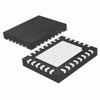
LTC3546IUFD#PBF Linear Technology, LTC3546IUFD#PBF Datasheet - Page 9

LTC3546IUFD#PBF
Manufacturer Part Number
LTC3546IUFD#PBF
Description
IC BUCK SYNC ADJ 1A/2A DL 28QFN
Manufacturer
Linear Technology
Type
Step-Down (Buck)r
Datasheet
1.LTC3546EUFDTRPBF.pdf
(28 pages)
Specifications of LTC3546IUFD#PBF
Internal Switch(s)
Yes
Synchronous Rectifier
Yes
Number Of Outputs
2
Voltage - Output
0.6 ~ 5 V
Current - Output
1A, 2A
Frequency - Switching
2.25MHz, 0.75MHz ~ 4MHz
Voltage - Input
2.25 ~ 5.5 V
Operating Temperature
-40°C ~ 125°C
Mounting Type
Surface Mount
Package / Case
28-QFN
Dc To Dc Converter Type
Step Down
Pin Count
28
Input Voltage
5.5V
Output Voltage
0.6 to 5V
Switching Freq
750 TO 4000/2900KHz
Output Current
2A
Efficiency
96%
Package Type
QFN EP
Output Type
Adjustable
Switching Regulator
Yes
Load Regulation
0.2%
Line Regulation
0.2%/V
Mounting
Surface Mount
Input Voltage (min)
2.25V
Operating Temperature Classification
Automotive
Lead Free Status / RoHS Status
Lead free / RoHS Compliant
Power - Output
-
Lead Free Status / Rohs Status
Compliant
Available stocks
Company
Part Number
Manufacturer
Quantity
Price
PIN FUNCTIONS
BMC2 (Pin 1/Pin 4): Burst Mode Clamp for Channel 2.
Connect-ing this pin to an external voltage between 0V and
0.6V sets the Burst Mode clamp level. If this pin is pulled
to V
TRACK/SS2 (Pin 2/Pin 5): Tracking input for Channel 2
output or optional external soft-start input. V
an external voltage at this pin. Leaving this pin fl oating
allows V
external soft-start can be programmed by connecting a
capacitor between this pin and ground. External soft-start
ramp time must be greater than the internal soft-start time
of 1.2ms. Refer to the Applications Information section
for more details.
V
tive divider from the Channel 2 regulator output. Nominal
voltage for this pin is 0.6V.
I
nel 2 Regulator. Peak current increases with an increase
in the voltage on this pin. Nominal voltage range for this
pin is 0V to 1.5V.
V
cuitry.
RUN2 (Pin 6/Pin 9): Low Level Logic Input. Enable for
Channel 2. When pulled high, regulator is running. When
at 0V, regulator is off. When both RUN1 and RUN2 are at
0V the part is in shutdown.
V
which connects from V
V
which connects from V
V
nel switch which connects from V
SW2A (Pin 10/Pin 13): Half of the switch node connec-
tion to the inductor for Channel 2. SW2A and SW2B must
be externally tied together. This pin swings from V
PGND2.
TH2
FB2
CCD
IN2
IN1
IN1D
CCA
(Pin 4/Pin 7): Error Amplifi er Compensation for Chan-
(Pin 7/Pin 10): Supply pin for 2A P-channel switch
(Pin 8/Pin 11): Supply pin for 1A P-channel switch
(Pin 3/Pin 6): Feedback voltage from external resis-
(Pin 5/Pin 8): Supply Pin for Internal Digital Cir-
(Pin 9/Pin 12): Supply pin for 1A dependent P-chan-
, an internal Burst Mode clamp level is used.
OUT2
to start-up using the internal soft-start. An
IN2
IN1
to SW2A/B.
to SW1.
(UFD/FE)
IN1D
to SW1D.
OUT2
will track
IN2
to
SW2B (Pin 11/Pin 14): Half of the switch node connec-
tion to the inductor for Channel 2 SW2A and SW2B must
be externally tied together. This pin swings from V
PGND2.
SW1D (Pin 12/Pin 15): The Dependent Switch Node
Connection. The pin is externally connected to SW1 for
a 2A/2A regulator or to SW2A/B for a 3A/1A regulator.
Internal circuitry detects which pin SW1D is externally
connected to, SW1 or SW2A/B. This pin swings from
V
by the output switch to which it is connected, i.e., SW1
or SW2A/SW2B. The dependant 1A power stage can be
disabled by fl oating the SW1D pin. The SW1D pin must
never be connected to V
is pulled high internally.
SW1 (Pin 13/Pin 16): The switch node connection to the
Inductor for the Channel 1 regulator. This pin swings from
V
PGND1D (Pin 14/Pin 17): Ground for SW1D Switching
N-Channel Driver.
PGND1 (Pin 15/Pin 18): Ground for SW1 Switching N-
Channel Driver.
PGND2 (Pin 16/Pin 19): Ground for SW2A and SW2B
Switching N-Channel Driver.
RUN1 (Pin 17/Pin 20): Low Level Logic Input. Enable for
Channel 1. When pulled high, regulator is running. When
at 0V, regulator is off. When both RUN1 and RUN2 are at
0V the part is in shutdown.
PHASE (Pin 18/Pin 21): Low Level Logic Input. Selects
Channel 2 regulator switching phase with respect to
Channel 1 regulator switching. When pulled high, the
SW1 regulator and the SW2A/B regulator are in phase.
When PHASE is at 0V the SW1 regulator and the SW2A/B
regulator are switching 180° out-of-phase.
I
Channel 1. Peak current increases with an increase in the
voltage on this pin. Nominal voltage range for this pin is
0V to 1.5V.
TH1
IN1D
IN1
to PGND1.
(Pin 19/Pin 22): Error Amplifi er Compensation for
to PGND1D. SW1D switching will be controlled
IN
or GND. When disabled, SW1D
LTC3546
IN2
3546fb
9
to


