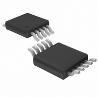
LTC1871EMS#PBF Linear Technology, LTC1871EMS#PBF Datasheet - Page 12

LTC1871EMS#PBF
Manufacturer Part Number
LTC1871EMS#PBF
Description
IC CONTRLR CURRENT MODE 10-MSOP
Manufacturer
Linear Technology
Type
Step-Up (Boost), Flyback, Sepicr
Datasheet
1.LTC1871EMS.pdf
(36 pages)
Specifications of LTC1871EMS#PBF
Internal Switch(s)
No
Synchronous Rectifier
No
Number Of Outputs
1
Voltage - Output
1.23 ~ 72 V
Current - Output
50mA
Frequency - Switching
50kHz ~ 1MHz
Voltage - Input
2.5 ~ 36 V
Operating Temperature
-40°C ~ 85°C
Mounting Type
Surface Mount
Package / Case
10-MSOP, Micro10™, 10-uMAX, 10-uSOP
Input Voltage
36V
Output Current
50mA
Output Voltage
12V
Supply Voltage Range
2.5V To 36V
No. Of Pins
10
Operating Temperature Range
-40°C To +85°C
Msl
MSL 1 - Unlimited
Rohs Compliant
Yes
Lead Free Status / RoHS Status
Lead free / RoHS Compliant
Power - Output
-
Available stocks
Company
Part Number
Manufacturer
Quantity
Price
LTC1871
APPLICATIONS INFORMATION
temperature rating. The junction temperature can be
estimated using the following equations:
The total quiescent current I
supply current (I
discharge the gate of the power MOSFET. The 10-pin MSOP
package has a thermal resistance of R
As an example, consider a power supply with V
V
and the maximum ambient temperature is 70°C. The power
MOSFET chosen is the IRF7805, which has a maximum
R
total gate charge of 37nC (the temperature coeffi cient of
the gate charge is low).
This demonstrates how signifi cant the gate charge current
can be when compared to the static quiescent current in
the IC.
To prevent the maximum junction temperature from being
exceeded, the input supply current must be checked when
operating in a continuous mode at high V
between the operating frequency and the size of the power
MOSFET may need to be made in order to maintain a reliable
IC junction temperature. Prior to lowering the operating
frequency, however, be sure to check with power MOSFET
manufacturers for their latest-and-greatest low Q
R
nologies are continually improving, with newer and better
performance devices being introduced almost yearly.
Output Voltage Programming
The output voltage is set by a resistor divider according
to the following formula:
12
O
DS(ON)
DS(ON)
I
P
T
I
P
T
V
= 12V at I
Q(TOT)
Q(TOT)
J
J
IC
IC
O
= T
= 70°C + 120°C/W • 95mW = 81.4°C
= 1.230V • 1+
= V
= 5V • 19.1mA = 95mW
of 11mΩ (at room temperature) and a maximum
A
devices. Power MOSFET manufacturing tech-
IN
≈ I
= 600μA + 37nC • 500kHz = 19.1mA
+ P
• (I
Q
O
IC
+ f • Q
= 1A. The switching frequency is 500kHz,
Q
• R
Q
+ f • Q
) and the current required to charge and
TH(JA)
G
R2
R1
G
)
Q(TOT)
consists of the static
TH(JA)
IN
= 120°C/W.
. A tradeoff
IN
= 5V and
G
, low
The external resistor divider is connected to the output
as shown in Figure 1, allowing remote voltage sensing.
The resistors R1 and R2 are typically chosen so that the
error caused by the current fl owing into the FB pin dur-
ing normal operation is less than 1% (this translates to a
maximum value of R1 of about 250k).
Programming Turn-On and Turn-Off Thresholds with
the RUN Pin
The LTC1871 contains an independent, micropower voltage
reference and comparator detection circuit that remains
active even when the device is shut down, as shown in
Figure 8. This allows users to accurately program an input
voltage at which the converter will turn on and off. The
falling threshold voltage on the RUN pin is equal to the
internal reference voltage of 1.248V. The comparator has
100mV of hysteresis to increase noise immunity.
The turn-on and turn-off input voltage thresholds are
programmed using a resistor divider according to the
following formulas:
The resistor R1 is typically chosen to be less than 1M.
For applications where the RUN pin is only to be used as
a logic input, the user should be aware of the 7V Absolute
Maximum Rating for this pin! The RUN pin can be con-
nected to the input voltage through an external 1M resistor,
as shown in Figure 8c, for “always on” operation.
Application Circuits
A basic LTC1871 application circuit is shown in Figure 1.
External component selection is driven by the character-
istics of the load and the input supply. The fi rst topology
to be analyzed will be the boost converter, followed by
SEPIC (single ended primary inductance converter).
V
V
IN(OFF)
IN(ON)
= 1.348V • 1+
= 1.248V • 1+
R2
R1
R2
R1
1871fe


