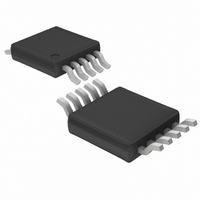
LTC1871EMS#PBF Linear Technology, LTC1871EMS#PBF Datasheet - Page 14

LTC1871EMS#PBF
Manufacturer Part Number
LTC1871EMS#PBF
Description
IC CONTRLR CURRENT MODE 10-MSOP
Manufacturer
Linear Technology
Type
Step-Up (Boost), Flyback, Sepicr
Datasheet
1.LTC1871EMS.pdf
(36 pages)
Specifications of LTC1871EMS#PBF
Internal Switch(s)
No
Synchronous Rectifier
No
Number Of Outputs
1
Voltage - Output
1.23 ~ 72 V
Current - Output
50mA
Frequency - Switching
50kHz ~ 1MHz
Voltage - Input
2.5 ~ 36 V
Operating Temperature
-40°C ~ 85°C
Mounting Type
Surface Mount
Package / Case
10-MSOP, Micro10™, 10-uMAX, 10-uSOP
Input Voltage
36V
Output Current
50mA
Output Voltage
12V
Supply Voltage Range
2.5V To 36V
No. Of Pins
10
Operating Temperature Range
-40°C To +85°C
Msl
MSL 1 - Unlimited
Rohs Compliant
Yes
Lead Free Status / RoHS Status
Lead free / RoHS Compliant
Power - Output
-
Available stocks
Company
Part Number
Manufacturer
Quantity
Price
LTC1871
APPLICATIONS INFORMATION
Boost Converter: Ripple Current ΔI
The constant ‘
percentage peak-to-peak ripple current in the inductor,
relative to its maximum value. For example, if 30% ripple
current is chosen, then
15% greater than the average.
For a current mode boost regulator operating in CCM,
slope compensation must be added for duty cycles above
50% in order to avoid subharmonic oscillation. For the
LTC1871, this ramp compensation is internal. Having an
internally fi xed ramp compensation waveform, however,
does place some constraints on the value of the inductor
and the operating frequency. If too large an inductor is
used, the resulting current ramp (ΔI
to the internal ramp compensation (at duty cycles above
50%), and the converter operation will approach voltage
mode (ramp compensation reduces the gain of the current
loop). If too small an inductor is used, but the converter
is still operating in CCM (near critical conduction mode),
the internal ramp compensation may be inadequate to
prevent subharmonic oscillation. To ensure good current
mode gain and avoid subharmonic oscillation, it is recom-
mended that the ripple current in the inductor fall in the
range of 20% to 40% of the maximum average current.
For example, if the maximum average input current is
1A, choose a ΔI
between 0.2 and 0.4.
Boost Converter: Inductor Selection
Given an operating input voltage range, and having chosen
the operating frequency and ripple current in the inductor,
the inductor value can be determined using the following
equation:
Remember that boost converters are not short-circuit
protected. Under a shorted output condition, the inductor
current is limited only by the input supply capability. For
14
where:
L =
I
L
V
= •
IN(MIN)
I
L
• f
1– D
I
O(MAX)
χ
• D
L
’ in the equation above represents the
MAX
between 0.2A and 0.4A, and a value ‘
MAX
χ
= 0.30, and the peak current is
L
) will be small relative
L
and the ‘
χ
’ Factor
χ
’
applications requiring a step-up converter that is short-
circuit protected, please refer to the applications section
covering SEPIC converters.
The minimum required saturation current of the inductor
can be expressed as a function of the duty cycle and the
load current, as follows:
The saturation current rating for the inductor should be
checked at the minimum input voltage (which results
in the highest inductor current) and maximum output
current.
Boost Converter: Operating in Discontinuous Mode
Discontinuous mode operation occurs when the load cur-
rent is low enough to allow the inductor current to run out
during the off-time of the switch, as shown in Figure 9.
Once the inductor current is near zero, the switch and diode
capacitances resonate with the inductance to form damped
ringing at 1MHz to 10MHz. If the off-time is long enough,
the drain voltage will settle to the input voltage.
Depending on the input voltage and the residual energy
in the inductor, this ringing can cause the drain of the
power MOSFET to go below ground where it is clamped
by the body diode. This ringing is not harmful to the IC
and it has not been shown to contribute signifi cantly to
EMI. Any attempt to damp it with a snubber will degrade
the effi ciency.
MOSFET DRAIN
I
L(SAT)
INDUCTOR
CURRENT
VOLTAGE
2A/DIV
2V/DIV
Figure 9. Discontinuous Mode Waveforms
V
V
IN
OUT
1+
= 3.3V I
= 5V
2
OUT
•
1– D
I
= 200mA
O(MAX)
MAX
2μs/DIV
1871 F09
1871fe


