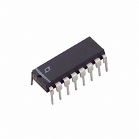
LTC1149CN-5 Linear Technology, LTC1149CN-5 Datasheet - Page 12

LTC1149CN-5
Manufacturer Part Number
LTC1149CN-5
Description
IC SW REG STEP-DOWN 5V 16-DIP
Manufacturer
Linear Technology
Type
Step-Down (Buck)r
Datasheet
1.LTC1149CNPBF.pdf
(20 pages)
Specifications of LTC1149CN-5
Internal Switch(s)
No
Synchronous Rectifier
Yes
Number Of Outputs
1
Voltage - Output
5V
Current - Output
50mA
Frequency - Switching
250kHz
Voltage - Input
0 ~ 48 V
Operating Temperature
0°C ~ 70°C
Mounting Type
Through Hole
Package / Case
16-DIP (0.300", 7.62mm)
Lead Free Status / RoHS Status
Contains lead / RoHS non-compliant
Power - Output
-
Available stocks
Company
Part Number
Manufacturer
Quantity
Price
Company:
Part Number:
LTC1149CN-5
Manufacturer:
LT
Quantity:
6 244
Part Number:
LTC1149CN-5#PBF
Manufacturer:
LINEAR/凌特
Quantity:
20 000
APPLICATIO S I FOR ATIO
LTC1149
LTC1149-3.3/LTC1149-5
the ground side of the output to prevent the absolute
maximum voltage ratings of the sense pins from being
exceeded. This is shown in Figure 5. When the current
sense comparator is operating at 0V common mode, the
off-time increases approximately 40%, requiring the use
of a smaller timing capacitor C
Efficiency Considerations
The percent efficiency of a switching regulator is equal to
the output power divided by the input power times 100%.
It is often useful to analyze individual losses to determine
what is limiting the efficiency and which change would
produce the most improvement. Percent efficiency can be
expressed as:
where L1, L2, etc., are the individual losses as a percent-
age of input power. (For high efficiency circuits only small
errors are incurred by expressing losses as a percentage
of output power.)
Although all dissipative elements in the circuit produce
losses, four main sources usually account for most of the
losses in LTC1149 series circuits: 1) LTC1149 DC supply
current, 2) MOSFET gate charge current, 3) I
4) P-channel transition losses.
1. The DC supply current is the current which flows into
2. MOSFET gate charge current results from switching the
12
%Efficiency = 100 – (L1 + L2 + L3 + ...)
V
LTC1149 DC supply current is 0.6mA for no load, and
increases proportionally with load up to 2mA after the
LTC1149 series has entered continuous mode.
Because the DC supply current is drawn from V
resulting loss increases with input voltage. For
V
for load currents over 300mA. However, at very low
load currents the DC bias current accounts for nearly all
of the loss.
gate capacitance of the power MOSFETs. Each time a
MOSFET gate is switched from low to high to low again,
a packet of charge dQ moves from V
resulting dQ/dt is a current out of V
much larger than the DC supply current. In continuous
IN
IN
Pin 2 less the gate charge current. For V
= 24V, the DC bias losses are generally less than 3%
U U
T
.
W
IN
IN
which is typically
to ground. The
2
R losses and
IN
= 12V the
U
IN
, the
3. I
4. Transition losses apply only to the P-channel MOSFET,
For example, if V
large MOSFET) and f = 100kHz, the transition loss is 0.7W.
A loss of this magnitude would not only kill efficiency but
would probably require additional heat sinking for the
MOSFET! See Design Example for further guidelines on
how to select the P-channel MOSFET.
Other losses including C
losses, Schottky conduction losses during dead-time, and
inductor core losses, generally account for less than 2%
total additional loss.
mode, I
for a 0.1 N-channel power MOSFET is 25nC, and for
a P-channel about twice that value. This results in
I
a 5% to 10% typical mid-current loss with V
Note that the gate charge loss increases directly with
both input voltage and operating frequency. This is the
principal reason why the highest efficiency circuits
operate at moderate frequencies. Furthermore, it
argues against using larger MOSFETs than necessary
to control I
as well as money!
of the MOSFET, inductor and current shunt. In continu-
ous mode all of the output current flows through L and
R
N-channel MOSFETs. If the two MOSFETs have
approximately the same R
one MOSFET can simply be summed with the resis-
tances of L and R
example, if each R
R
results in losses ranging from 3% to 12% as the output
current increases from 0.5A to 2A. I
efficiency to roll-off at high output currents.
and only when operating at high input voltages (typi-
cally 24V or greater). Transition losses can be esti-
mated from:
Transition Loss 5(V
GATECHG
2
SENSE
SENSE
R losses are easily predicted from the DC resistances
, but is “chopped” between the P-channel and
= 0.05 , then the total resistance is 0.3 . This
GATECHG
= 7.5mA in 100kHz continuous operation, for
2
R losses, since overkill can cost efficiency
IN
= 48V, I
= f (Q
DS(ON)
SENSE
IN
N
MAX
IN
)
+ Q
2
DS(ON)
(I
and C
to obtain I
MAX
= 0.1 , R
P
= 2A, C
). The typical gate charge
)(C
, then the resistance of
OUT
RSS
2
RSS
R losses cause the
)(f)
ESR dissipative
L
2
= 300pF (a very
R losses. For
= 0.15
IN
= 24V.
and


