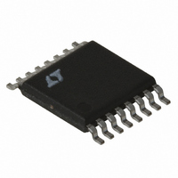
LT1976IFE#TR Linear Technology, LT1976IFE#TR Datasheet - Page 21

LT1976IFE#TR
Manufacturer Part Number
LT1976IFE#TR
Description
IC REG SW STEP DWN 1.5A 16-TSSOP
Manufacturer
Linear Technology
Type
Step-Down (Buck)r
Datasheet
1.LT1976IFEPBF.pdf
(28 pages)
Specifications of LT1976IFE#TR
Internal Switch(s)
Yes
Synchronous Rectifier
No
Number Of Outputs
1
Voltage - Output
1.2 ~ 54 V
Current - Output
1.5A
Frequency - Switching
200kHz
Voltage - Input
3.3 ~ 60 V
Operating Temperature
-40°C ~ 125°C
Mounting Type
Surface Mount
Package / Case
16-TSSOP Exposed Pad, 16-eTSSOP, 16-HTSSOP
Lead Free Status / RoHS Status
Contains lead / RoHS non-compliant
Power - Output
-
Available stocks
Company
Part Number
Manufacturer
Quantity
Price
See the Typical Performance Characteristics section for
graphs of SHDN and V
SYNCHRONIZING
Oscillator synchronization to an external input is achieved
by connecting a TTL logic-compatible square wave with a
duty cycle between 20% and 80% to the LT1976 SYNC
pin. The synchronizing range is equal to initial operating
frequency up to 700kHz. This means that minimum
practical sync frequency is equal to the worst-case high
self-oscillating frequency (230kHz), not the typical oper-
ating frequency of 200kHz. Caution should be used when
synchronizing above 230kHz because at higher sync
frequencies the amplitude of the internal slope compen-
sation used to prevent subharmonic switching is re-
duced. This type of subharmonic switching only occurs at
input voltages less than twice output voltage. Higher
inductor values will tend to eliminate this problem. See
Frequency Compensation section for a discussion of an
entirely different cause of subharmonic switching before
assuming that the cause is insufficient slope compensa-
tion. Application Note 19 has more details on the theory
of slope compensation.
If the FB pin voltage is below 0.9V (power-up or output
short-circuit conditions) the sync function is disabled.
This allows the frequency foldback to operate to avoid and
hazardous conditions for the SW pin.
APPLICATIO S I FOR ATIO
U
IN
V
OUT
currents verses input voltage.
U
R3
R1
R2
W
15
4
LT1976
V
SHDN
IN
3μA
Figure 8. Undervoltage Lockout
2.4V
1.3V
U
–
–
+
+
COMP
SHDN
COMP
V
IN
If the synchronization signal is present during Burst Mode
operation, synchronization will occur during the burst
portion of the output waveform. Synchronizing the LT1976
during Burst Mode operation may alter the natural burst
frequency which can lead to jitter and increased ripple in
the burst waveform. Synchronizing the LT1976B during
pulse skip operation may also increase output ripple.
If no synchronization is required this pin should be con-
nected to ground.
POWER GOOD
The LT1976 contains a power good block which consists
of a comparator, delay timer and active low flag that allows
the user to generate a delayed signal after the power good
threshold is exceeded.
Referring to Figure 2, the PGFB pin is the positive input to
a comparator whose negative input is set at V
PGFB is taken above V
the C
the PGFB pin drops below V
discharged resetting the delay period. The PGFB voltage is
typically generated by a resistive divider from the regu-
lated output or input supply.
The capacitor on the C
delay time between the PGFB pin exceeding its threshold
(V
When the PGFB pin rises above V
PGFB
T
) and the PG pin set to a high impedance state.
pin starting the delay period. When the voltage on
ENABLE
1976 F08
PGFB
T
LT1976/LT1976B
pin determines the amount of
, current (I
PGFB
PGFB
the C
CSS
current is sourced
) is sourced into
T
pin is rapidly
PGFB
21
. When
1976bfg


