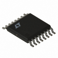
LT1976IFE#TR Linear Technology, LT1976IFE#TR Datasheet - Page 24

LT1976IFE#TR
Manufacturer Part Number
LT1976IFE#TR
Description
IC REG SW STEP DWN 1.5A 16-TSSOP
Manufacturer
Linear Technology
Type
Step-Down (Buck)r
Datasheet
1.LT1976IFEPBF.pdf
(28 pages)
Specifications of LT1976IFE#TR
Internal Switch(s)
Yes
Synchronous Rectifier
No
Number Of Outputs
1
Voltage - Output
1.2 ~ 54 V
Current - Output
1.5A
Frequency - Switching
200kHz
Voltage - Input
3.3 ~ 60 V
Operating Temperature
-40°C ~ 125°C
Mounting Type
Surface Mount
Package / Case
16-TSSOP Exposed Pad, 16-eTSSOP, 16-HTSSOP
Lead Free Status / RoHS Status
Contains lead / RoHS non-compliant
Power - Output
-
Available stocks
Company
Part Number
Manufacturer
Quantity
Price
LT1976/LT1976B
APPLICATIO S I FOR ATIO
Board layout also has a significant effect on thermal
resistance. Pin 8 and the exposed die pad, Pin 17, are a
continuous copper plate that runs under the LT1976 die.
This is the best thermal path for heat out of the package.
Reducing the thermal resistance from Pin 8 and exposed
pad onto the board will reduce die temperature and in-
crease the power capability of the LT1976. This is achieved
by providing as much copper area as possible around the
exposed pad. Adding multiple solder filled feedthroughs
under and around this pad to an internal ground plane will
also help. Similar treatment to the catch diode and coil
terminations will reduce any additional heating effects.
THERMAL CALCULATIONS
Power dissipation in the LT1976 chip comes from four
sources: switch DC loss, switch AC loss, boost circuit
current, and input quiescent current. The following formu-
las show how to calculate each of these losses. These
formulas assume continuous mode operation, so they
should not be used for calculating efficiency at light load
currents.
Switch loss:
Boost current loss:
Quiescent current loss: (LT1976)
R
t
(t
t
t
t
f = switch frequency
24
EFF
r
f
IR
SW
r
= (V
= (V
P
P
P
+ t
= t
BOOST
SW
Q
= effective switch current/voltage overlap time
f
= switch resistance (≈0.3 when hot )
IF
= V
IN
IN
+ t
=
= (I
/1.7)ns
/1.2)ns
IN
IR
R
=
OUT
SW OUT
(0.0015) + V
+ t
(
V
IF
(
/0.05)ns
OUT
I
)
V
U
IN
) (
) (
2
V
2
IN
I
OUT
V
OUT
OUT
U
/
36
)
(0.003)
+
)
t
EFF
W
( ) (
1 2 /
I
OUT
U
)( )( )
V
IN
f
Example: with V
Total power dissipation is:
Thermal resistance for the LT1976 package is influenced
by the presence of internal or backside planes. With a full
plane under the FE16 package, thermal resistance will be
about 45°C/W. No plane will increase resistance to about
150°C/W. To calculate die temperature, use the proper
thermal resistance number for the desired package and
add in worst-case ambient temperature:
With the FE16 package (Q
temperature of 70°C:
If a more accurate die temperature is required, a measure-
ment of the SYNC pin resistance to ground can be used.
The SYNC pin resistance can be measured by forcing a
voltage no greater than 0.25V at the pin and monitoring the
pin current versus temperature in a controlled temperature
environment. The measurement should be done with
minimal device power dissipation (pull the V
ground for sleep mode) in order to calibrate the SYNC pin
resistance with the ambient temperature.
P
T
T
P
P
P
0 04 0 388 0 43
BOOST
J
J
SW
Q
TOT
.
= T
= 70 + 45(0.53) = 94°C
=
=
= 0.43 + 0.02 + 0.08 = 0.53W
+
40 0 0015
A
( )( ) ( )
+ Q
=
0 3 1 5
(
.
.
( ) (
.
JA
5
40
IN
2
(P
=
40
2
1 36
= 40V, V
TOT
)
/
.
+
)
)
5 0 003
+
W
(
=
(
97
.
0 02
OUT
JA
.
e
–
= 45°C/W) at an ambient
)
W
= 5V and I
9 1 2 1 40 200 3
=
) ( ) ( )( )(
0 08
.
/
W
OUT
= 1A:
C
pin to
e
1976bfg
)


