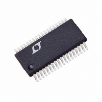
LTC1876EG#TR Linear Technology, LTC1876EG#TR Datasheet - Page 29

LTC1876EG#TR
Manufacturer Part Number
LTC1876EG#TR
Description
IC CTRLR/REG STEP UP/DOWN 36SSOP
Manufacturer
Linear Technology
Series
PolyPhase®r
Type
Step-Down (Buck), Step-Up (Boost)r
Datasheet
1.LTC1876EGPBF.pdf
(36 pages)
Specifications of LTC1876EG#TR
Internal Switch(s)
No
Synchronous Rectifier
Yes
Number Of Outputs
3
Voltage - Output
Adj to 34V
Current - Output
1A
Frequency - Switching
140kHz ~ 340kHz
Voltage - Input
3.5 ~ 36 V
Operating Temperature
-40°C ~ 85°C
Mounting Type
Surface Mount
Package / Case
36-SSOP
Lead Free Status / RoHS Status
Contains lead / RoHS non-compliant
Power - Output
-
Available stocks
Company
Part Number
Manufacturer
Quantity
Price
APPLICATIO S I FOR ATIO
Choosing 1% resistors; R1 = 25.5k and R2 = 32.4k yields
an output voltage of 1.816V.
The power dissipation on the top side MOSFET can be
easily estimated. Choosing a Siliconix Si4412DY results
in; R
voltage with T(estimated) = 50 C:
A short-circuit to ground will result in a folded back
current of:
with a typical value of R
= 0.1. The resulting power dissipated in the bottom
MOSFET is:
which is less than under full-load conditions.
C
temperature assuming only this channel is on. C
chosen with an ESR of 0.02 for low output ripple. The
output ripple in continuous mode will be highest at the
maximum input voltage. The output voltage ripple due to
ESR is approximately:
Design Example for Auxiliary Regulator
Assume the requirements are V
I
P
OUTMAX
SYNC
IN
V
P
I
Duty Cycle
SC
is chosen for an RMS current rating of at least 3A at
MAIN
ORIPPLE
DS(ON)
= 300mA. The duty cycle is given by:
25
0 01
434
22
.
0 042
= 0.042 , C
220
1 8
mV
V
22
= R
.
22
.
mW
– .
V
V
mW
V
ESR
1 8
1
5 1 0 005 50
–
2
1
( I
V
U
2
V
V
200
OUT
3 2
L
1 7 22
IN
) = 0.02 (1.67A) = 33mV
.
.
RSS
3 3
A
( .
ns
DS(ON)
.
U
2
(
= 100pF. At maximum input
22
0 58
V
H
1 1 0 042
.
V
.
2
)(
IN
and
)
5
= 5V, V
A
W
.
C
3 2
100
.
= (0.005/ C)(20)
–
A
25
OUT
pF
C
= 12V and
300
U
)
P–P
OUT
kHz
is
Since the required output current is 300mA, the ripple
current of the inductor is calculated to be 0.57A.
Hence the required inductor is:
With the boost regulator operating at 1.2MHz,
A 10 H inductor is selected for the circuit for lower ripple
inductor current. Since the output current is only 300mA,
a 0.5A MBR0520 Schottky is selected. The completed
circuit along with its efficiency curve is shown in Figure 13
and Figure 14 respectively.
2.2 F
L = 4.24 H
V
L
C
IN3
5V
IN3
(
Figure 14. Efficiency Curve for Design Example
V
C1: TAIYO YUDEN X5R LMK212BJ225MG
C2: TAIYO YUDEN X5R EMK316BJ475ML
D1: ON SEMICONDUCTOR MBR0520
L1: SUMIDA CR43-100
*OPTIONAL
IN
SHDN
•
Figure 13. Design Example Schematic
( •
90
85
80
75
70
65
60
55
50
Duty Cycle
f
0
AUXV
AUXSD AUXV
I
L
LTC1876
)
IN
10 H
SGND
100
L3
AUXSW
LOAD CURRENT (mA)
)
FB
V
IN
200
= 3.3V
R8
113k
R7
13.3k
D1
V
IN
300
= 5V
C3*
10pF
LTC1876
1876 F14
+
400
C
4.7 F
V
12V
300mA
1876 F13
OUT3
OUT3
29
1876fa


