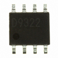
BD9322EFJ-E2 Rohm Semiconductor, BD9322EFJ-E2 Datasheet

BD9322EFJ-E2
Specifications of BD9322EFJ-E2
Available stocks
Related parts for BD9322EFJ-E2
BD9322EFJ-E2 Summary of contents
Page 1
... Integrated Compensation BD9322EFJ, BD9323EFJ, BD9324EFJ Description The BD9322EFJ, BD9323EFJ and BD9324EFJ are step-down regulators that integrate a low resistance high side N-channel MOSFET. It achieves continuous output current over a wide input supply range. Current mode operation provides fast transient response and easy phase compensation. ...
Page 2
... Hi-side FET On-resistance for BD9323EFJ Hi-side FET On-resistance for BD9324EFJ Lo-side FET On-resistance Leak current N-channel Switch Current Limit for BD9322EFJ Switch Current Limit for BD9323EFJ Switch Current Limit for BD9324EFJ Maximum duty cycle General Enable Pull-up current Enable Threshold voltage ...
Page 3
Block Diagram VIN OPEN EN AUTOMATIC VREF STARTUP IBIAS + FB ERR - COMP SS SoftStart ● Typical Application Circuit VIN 12V C_VC1 10μF 5V OSC VREG OCP UVLO TSD LVS S DRV LOGIC + SLOPE PWM LVS R ...
Page 4
Block Operation •VREG A block to generate constant-voltage for DC/DC boosting. •VREF A block that generates internal reference voltage of 2.9 V (Typ.). •TSD/UVLO TSD (Thermal shutdown)/UVLO (Under Voltage Lockout) protection block. The TSD circuit shuts down IC at 175℃ ...
Page 5
Physical Dimension Pin Assignment and Pin Function Pin No 4.9±0.1 (Max5.25 include.BURR) (3. 0.545 1PIN MARK S +0.05 0.42 0.08 1.27 M -0.04 0.08 ...
Page 6
... Iout [A] Fig. STEP Down Efficiency (VIN= 12V V = 3.3V L= 22uH) OUT 200 180 160 140 120 100 VIN : [V] Fig. Quiescent Current 0.25 0.2 BD9322EFJ 0.15 0.1 BD9323/24EFJ 0.05 0 -40 - [℃] Fig. Hi-Side On-resistance V OUT OUT 2 Fig. OverCurrent Protection (V is shorted to GND) OUT 6/13 0 ...
Page 7
V V -MAX: +120mV OUT V OUT V -MIN: -100m V OUT Div OUT I OUT Fig. Transient Response (VIN= 12V V = 3.3V L= 10uH Cout =22uF Iout= 0.2-1.0A ) OUT V : 200 ...
Page 8
Selecting Application Components (1) Output LC constant (Buck Converter) The inductance L to use for output is decided by the rated current I inductance. IL Fig. Adjust so that I + ∆I OMAX equation. 1 × (Vcc - Vo) × ...
Page 9
Compensation Choosing compensation capacitor C The example of DC/DC converter application bode plot is shown below. The compensation resistor R F that decides the stability and response speed of DC/DC converter. So compensation resistor R C for good stability ...
Page 10
Design of Feedback Resistance constant Set the feedback resistance as shown below Soft Start Function COMP ERRAMP 2.9V(typ Function VIN VIN + EN The equivalent internal circuit. ex) The example of EN driving ...
Page 11
Layout Pattern Consideration Two high pulsing current flowing loops exist in the buck regulator system. The first loop, when FET is ON, starts from the input capacitors, to the VIN terminal, to the SW terminal, to the inductor, to the ...
Page 12
Operation Notes 1) Absolute maximum ratings Use of the IC in excess of absolute maximum ratings such as the applied voltage or operating temperature range may result in IC damage. Assumptions should not be made regarding the state of the ...
Page 13
I/O Equivalent Circuit Diagram Fig. 1.SS VIN 6.FB VIN Power Dissipation (4)3760mW 4000 3000 (3)2110mW 2000 (2)1100mW 1000 (1)820mW AMBIENT TEMPERATURE: Ta [°C] 2.BST REG SW 7.COMP VIN VIN On 70 × 70 × 1.6 mm ...
Page 14
Appendix No technical content pages of this document may be reproduced in any form or transmitted by any means without prior permission of ROHM CO.,LTD. The contents described herein are subject to change without notice. The specifications for the product ...


