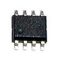
BD9327EFJ-E2 Rohm Semiconductor, BD9327EFJ-E2 Datasheet

BD9327EFJ-E2
Specifications of BD9327EFJ-E2
Available stocks
Related parts for BD9327EFJ-E2
BD9327EFJ-E2 Summary of contents
Page 1
... Built-in Power MOSFET BD9325FJ,BD9326EFJ,BD9327EFJ ●Description The BD9325FJ, BD9326EFJ and BD9327EFJ are step-down regulators that integrate a low resistance high side N-channel MOSFET. It achieves continuous output current over a wide input supply range. Current mode operation provides fast transient response and easy phase compensation. ...
Page 2
... Hi-side FET On-resistance for BD9326EFJ Hi-side FET On-resistance for BD9327EFJ Lo-side FET On-resistance Leak current N-channel Switch Current Limit for BD9325FJ Switch Current Limit for BD9326EFJ Switch Current Limit for BD9327EFJ Maximum duty cycle General Enable Sink current Enable Threshold voltage Under Voltage Lockout threshold ...
Page 3
... IBIAS TSD S DRV LOGIC SLOPE + R PWM - GND Fig.1 Block Diagram C_PC1 3300pF R_PC C_SS 15k 0.1μF Thermal Pad (For BD9326EFJ, BD9327EFJ) D Fig.2 Application Circuit 3/14 Technical Note BST OCP 12V VIN LVS SW LVS R_DW 10k R_UP 27k L V 3.3V OUT 10μ ...
Page 4
... BD9325FJ, BD9326EFJ, BD9327EFJ ●Block operation ・VREG A block to generate constant-voltage for DC/DC boosting. ・VREF A block that generates internal reference voltage of 2.9 V (Typ.). ・TSD/UVLO TSD (Thermal shutdown)/UVLO (Under Voltage Lockout) protection block. The TSD circuit shuts down IC at 175℃ (Typ.) The UVLO circuit shuts down the IC when the VCC is Low Voltage. ...
Page 5
... BD9325FJ, BD9326EFJ, BD9327EFJ ●Typical performance characteristics (Unless otherwise specified, V 2.5 2.4 2.3 2.2 2.1 2 1.9 1.8 1.7 1.6 1 VIN : [V] Fig.3 Circuit Current (No switching) 0.923 0.913 0.903 0.893 0.883 0.873 -40 - 100 TEMPERATURE : [C] Fig.6 Feedback voltage 95 BD9326EFJ 90 BD9325FJ 0.2 0.4 0.6 0.8 1 1.2 1 ...
Page 6
... BD9325FJ, BD9326EFJ, BD9327EFJ V OUT V -MAX: +100mV OUT V OUT V -MIN: -100m V OUT I OUT I OUT Fig.12 Transient Response (VIN= 12V VOUT= 3.3V L= 10µH Cout =22µF Iout= 0.2-1. -MAX: +460mV OUT V OUT V -MIN: -240mV OUT Div OUT I OUT Fig.14 Transient Response (VIN= 12V V = 3.3V L= 10µ ...
Page 7
... BD9325FJ, BD9326EFJ, BD9327EFJ ●Selecting application components (1) Output LC constant (Buck Converter) The inductance L to use for output is decided by the rated current ILR and input current maximum value IOMAX of the inductance Fig.17 Adjust so that IOMAX + ∆IL does not reach the rated current value ILR. At this time, ∆IL can be obtained by the following equation ...
Page 8
... BD9325FJ, BD9326EFJ, BD9327EFJ (2) Loop Compensation Choosing compensation capacitor C The example of DC/DC converter application bode plot is shown below. The compensation resistor R3 will set the cross over frequency FC that decides the stability and response speed of DC/DC converter. So compensation resistor R3 has to be adjusted to adequate value for good stability and response speed. ...
Page 9
... BD9325FJ, BD9326EFJ, BD9327EFJ (3) Design of Feedback Resistance constant Set the feedback resistance as shown below. Reference voltage V OUT + R1 ERR - ●Soft Start Function COMP 2.9V(typ) ERRAMP + - ●EN Function VIN EN 66kΩ(typ.) Fig.19 The equivalent internal circuit. www.rohm.com © 2010 ROHM Co., Ltd. All rights reserved. ...
Page 10
... BD9325FJ, BD9326EFJ, BD9327EFJ ●Layout Pattern Consideration Two high pulsing current flowing loops exist in the buck regulator system. The first loop, when FET is ON, starts from the input capacitors, to the VIN terminal, to the SW terminal, to the inductor, to the output capacitors, and then returns to the input capacitor through GND. ...
Page 11
... BD9325FJ, BD9326EFJ, BD9327EFJ ●Operation Notes 1) Absolute maximum ratings Use of the IC in excess of absolute maximum ratings such as the applied voltage or operating temperature range may result in IC damage. Assumptions should not be made regarding the state of the IC (short mode or open mode) when such damage is suffered. A physical safety measure such as a fuse should be implemented when use of the special mode where the absolute maximum ratings may be exceeded is anticipated ...
Page 12
... BD9325FJ, BD9326EFJ, BD9327EFJ 10) Thermal shutdown circuit (TSD) This IC incorporates a built-in TSD circuit for the protection from thermal destruction. The IC should be used within the specified power dissipation range. However, in the event that the IC continues to be operated in excess of its power dissipation limits, the attendant rise in the chip's junction temperature Tj will trigger the TSD circuit to turn off all output power elements ...
Page 13
... BD9325FJ, BD9326EFJ, BD9327EFJ ●Power Dissipation 4000 (4)3760mW 3000 (3)2110mW 2000 (2)1100mW 1000 (1)820mW AMBIENT TEMPERATURE: Ta [°C] 4000 3000 2000 1000 (1)675mW AMBIENT TEMPERATURE: Ta [°C] www.rohm.com © 2010 ROHM Co., Ltd. All rights reserved. HTSOP-J8 Package On 70 70 1.6 mm glass epoxy PCB (1) 1-layer board (Backside copper foil area 0 mm ...
Page 14
... BD9325FJ, BD9326EFJ, BD9327EFJ ●Ordering part number Part No. Part No. 9325 9326 9327 SOP-J8 4.9±0.2 (MAX 5.25 include BURR) + 6° 4° −4° 0.545 0.2±0.1 S 1.27 0.42±0.1 0.1 S HTSOP-J8 4.9±0.1 (MAX 5.25 include BURR) (3.2) + 6° 4° −4° ...
Page 15
No copying or reproduction of this document, in part or in whole, is permitted without the consent of ROHM Co.,Ltd. The content specified herein is subject to change for improvement without notice. The content specified herein is for the purpose ...


