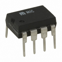
MIC3172YN Micrel Inc, MIC3172YN Datasheet - Page 10

MIC3172YN
Manufacturer Part Number
MIC3172YN
Description
IC REG SW 100KHZ 1.25A 8-DIP
Manufacturer
Micrel Inc
Type
Step-Down (Buck), Step-Up (Boost), Inverting, Cukr
Specifications of MIC3172YN
Internal Switch(s)
Yes
Synchronous Rectifier
No
Number Of Outputs
1
Current - Output
1.25A
Frequency - Switching
100kHz
Voltage - Input
3 ~ 40 V
Operating Temperature
-40°C ~ 85°C
Mounting Type
Through Hole
Package / Case
8-DIP (0.300", 7.62mm)
Power - Output
302mW
Primary Input Voltage
40V
No. Of Outputs
1
Output Current
3A
No. Of Pins
8
Operating Temperature Range
-40°C To +85°C
Supply Voltage Range
3V To 40V
Termination Type
Through Hole
Lead Free Status / RoHS Status
Lead free / RoHS Compliant
Voltage - Output
-
Lead Free Status / RoHS Status
Lead free / RoHS Compliant, Lead free / RoHS Compliant
Other names
576-2255
MIC3172YN
MIC3172YN
MIC2172/3172
Figure 7 shows how one or more MIC2172s can be locked to
an external reference frequency. The slaves lock to the
negative (falling edge) of the external reference waveform.
Soft Start
A diode-coupled capacitor from COMP to circuit ground
slows the output voltage rise at turn on (figure 8).
The additional time it takes for the error amplifier to charge the
capacitor corresponds to the time it takes the output to reach
regulation. Diode D1 discharges C1 when V
Current Limit
For designs demanding less output current than the MIC2172/
3172 is capable of delivering, P GND 1 can be left open
reducing the current capability of Q1 by one-half.
Alternatively, the maximum current limit of the MIC2172/3172
can be reduced by adding a voltage clamp to the COMP
output (figure 9). This feature can be useful in applications
requiring either a complete shutdown of Q1’s switching action
or a form of current fold-back limiting. This use of the COMP
output does not disable the oscillator, amplifiers or other
circuitry, therefore the supply current is never less than
approximately 5mA.
Thermal Management
Although the MIC2172/3172 family contains thermal protec-
tion circuitry, for best reliability, avoid prolonged operation
with junction temperatures near the rated maximum.
The junction temperature is determined by first calculating
the power dissipation of the device. For the MIC2172/3172,
M9999-042205
V
IN
Q1
V
P1 P2 S
IN
Figure 9. Current Limit
MIC2172/3172
GND
C1
R1
R2
D1
Figure 8. Soft Start
V
IN
COMP
V
FB
R3
SW
D2
C1
C2
MIC2172/3172
Note: Input and output
V
I
CL
IN
returns not common.
≈ 0.6V/R2
COMP
R1
C2
V
IN
OUT
is removed.
10
the total power dissipation is the sum of the device operating
losses and power switch losses.
The device operating losses are the dc losses associated
with biasing all of the internal functions plus the losses of the
power switch driver circuitry. The dc losses are calculated
from the supply voltage (V
The MIC2172/3172 supply current is almost constant regard-
less of the supply voltage (see “Electrical Characteristics”).
The driver section losses (not including the switch) are a
function of supply voltage, power switch current, and duty
cycle.
where:
As a practical example refer to figure 1.
Then:
Power switch dissipation calculations are greatly simplified
by making two assumptions which are usually fairly accurate.
First, the majority of losses in the power switch are due to
on-losses. To find these losses, assign a resistance value to
the collector/emitter terminals of the device using the satura-
tion voltage versus collector current curves (see Typical
Performance Characteristics).
calculated by modeling the switch as a resistor with the switch
duty cycle modifying the average power dissipation.
From the Typical performance Characteristics:
P
(bias+driver)
P
V
I
I
δ = duty cycle
V
I
I
δ = 60% (0.6)
P
P
R
P
Q
SW
Q
SW
(bias+driver)
IN
IN
(bias+driver)
SW
(bias+driver)
SW
= quiescent supply current
= 0.006A
= supply voltage
= 5.0V
= power switch current
= 0.625A
= (I
= 1Ω
(see “ Design Hints: Switch Current
V
V
δ =
Calculations”)
OUT
F
SW
= D1 forward voltage drop
= 5 × 0.006
V
)
OUT
= output voltage
(
2
= device operating losses
= 0.068W
= V
V
R
(
OUT
SW
+ V
IN
δ
IN
I
+ V
Q
F
) and device supply current (I
)
)
± V
+ 5 0.625
F
+ V
IN
IN
Power switch losses are
I
SW
0.004 + δ
0.004 + 0.6
50
50
Micrel, Inc.
April 2005
Q
).


