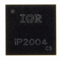
IP2004TR International Rectifier, IP2004TR Datasheet

IP2004TR
Specifications of IP2004TR
Related parts for IP2004TR
IP2004TR Summary of contents
Page 1
... The only additional components required for a complete multiphase converter are a PWM controller, the output inductors, and the input and output capacitors. Description iP2004 iP2004TR ENABLE PWM P GND ...
Page 2
Absolute Maximum Ratings V to PGND ……………………..…….…. -0.5V to 16V PGND …………………….….……. -0.5V to 6.5V DD PWM to PGND ………………….………… -0. ENABLE to PGND ………………………... -0. Storage Temperature …………..…………. -60ºC to 150ºC Block ...
Page 3
PARAMETER VDD Supply Current (Stand By) Supply Current (Operating) Power-On Reset (POR) VCC Rising Hysterisis ENABLE INPUT Logic Level Low Threshold ( Logic Level High Threshold ( Threshold Hysterisis Weak pull-down current Rising Propagation Delay (T ...
Page 4
Power Loss Curve 12V 5. 1. 1MHz 300nH 125ºC BLK ...
Page 5
Typical Performance Curves 1.40 1.35 1.30 1.25 1.20 1.15 1.10 1.05 1.00 0.95 0. Input Voltage (V) Figure 3 Normalized Power Loss vs. Input Voltage 1.06 1.04 1.02 1.00 0.98 0.96 0.94 0.92 4.50 ...
Page 6
... It incorporates the ability to solve thermal problems where heat is drawn out through the printed circuit board and the top of the case. Please refer to International Rectifier Application Note AN1047 for further details on using this SOA curve in your thermal environment. ...
Page 7
Calculating Power Loss and SOA for Different Operating Conditions To calculate Power Loss for a given set of operation conditions, the following procedure should be followed: Power Loss Procedure 1. Determine the maximum current for each iP2004 and obtain the ...
Page 8
Calculating SOA Temperature: (Figure 3) (Figure 4) (Figure 5) (Figure 6) (Figure 7) TX axis intercept adjustment ≈ -0.5 ºC + 5.5 ºC - 0.8 ºC + 0.6 ºC - 1.9 ºC ≈ 2.9 ºC Assuming T = 95ºC & ...
Page 9
NC 2 ENABLE 3 PWM GND Pin Description Pin Number Pin Name ENABLE 3 PWM PGND SWS1 9 ...
Page 10
Package Pinout Diagram ENABLE 2 PWM Page SWS1 8 SWS2 9 P GND 10 Figure 13 Top Side Transparent View www.irf.com Data Sheet No. PD60322 iP2004 ...
Page 11
Recommended PCB Layout Figure 14 Top copper and Solder-mask layer of PCB layout Page www.irf.com Data Sheet No. PD60322 iP2004 12/22/2007 ...
Page 12
... The following guidelines are recommended to reduce the parasitic values and optimize overall performance. • All pads on the iP2004 footprint design need to be Solder-mask defined (see International Rectifier application notes AN1028 and AN1029 for further footprint design guidance. • Place as many vias around the Power pads (V performance ...
Page 13
Mechanical Outline Drawing 0.15 [.006] C 7.65 [0.301] CORNER ID TOP VIEW 6.303 5.795 4.779 0.334 4.132 0.322 1.858 2.379 5.300 5.821 7.345 BOTTOM VIEW GND BOTTOM VIEW ELECTRICAL I/O Page 13 ...
Page 14
Recommended Solder Paste Stencil Design NOTES: 1. This view is stencil squeegee view 2. Dimensions are shown in millimeters 3. These openings are based on using a 150 micron thick stencil. If using different thickness stencil, this opening needs to ...
Page 15
Part Marking IR WORLD HEADQUARTERS: 233 Kansas St., El Segundo, California 90245, USA Tel: (310) 252-7105 Page Figure 19 Part Marking Data and specifications subject to change without notice. Visit us at www.irf.com www.irf.com Data Sheet No. ...


