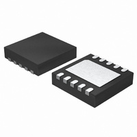
ISL97702IRZ-T7 Intersil, ISL97702IRZ-T7 Datasheet - Page 9

ISL97702IRZ-T7
Manufacturer Part Number
ISL97702IRZ-T7
Description
IC BOOST REG DUAL FEEDBACK 10DFN
Manufacturer
Intersil
Type
Step-Up (Boost)r
Datasheet
1.ISL97702IRZ.pdf
(13 pages)
Specifications of ISL97702IRZ-T7
Internal Switch(s)
Yes
Synchronous Rectifier
No
Number Of Outputs
2
Voltage - Output
Adj to 28V
Current - Output
130mA
Frequency - Switching
1MHz
Voltage - Input
2.3 ~ 5.5 V
Operating Temperature
-40°C ~ 85°C
Mounting Type
Surface Mount
Package / Case
10-DFN
Lead Free Status / RoHS Status
Lead free / RoHS Compliant
Power - Output
-
Fault Control
The input voltage at VDD, current in the VDDOUT switch,
voltage at V
continuously monitored and can either restart the start-up
sequence or in some cases disable the ISL97702 boost
function as long as the fault is present.
Maximum Duty Cycle – LX
The maximum duty cycle Dmax, at which the power FET can
operate defines the upper limit of the regulator output to
input voltage ratio according to the formula: V
(1-Dmax). In the ISL97702, Dmax is defined from the
minimum off-time toff(LX)min and the switching frequency.
Undervoltage at
VDD
Overcurrent drawn
from VDDOUT
Overvoltage at
VOUT
Over Temperature
on chip
DESCRIPTION
FAULT
OUT
TABLE 1. FAULT PROTECTION
and junction temperature Tj are
V(VDD) <
V(VDD)off
I(VDDOUT) >
It(VDDOUT)err
V(VOUT) >
Vt(VOUT)err
Tj > Toff
CONDITION
FAULT
FIGURE 16.
9
Disables I/Os and waits until
V(VDD) reaches V(VDD)on
to begin with the start-up
sequence
Disables VDDOUT switch
and LX driver and
immediately restarts the
start-up sequence
Disables VDDOUT switch
and LX driver and waits until
output voltage V(VOUT)
drops to Vt(VOUT) to restart
the start-up sequence
Disables VDDOUT switch
and LX driver and waits until
junction temp drops to “Ton”
to restart the start-up
sequence
ISL97702 FAULT
REACTION
OUT
/V
IN
= 1/
ISL97702
If NSYNC is tied to VDD the internal oscillator defines Dmax
to:
Dmax(fosc) = 1 - toff(LX)min*fosc
With external synchronization at pin NSYNC
Dmax(NSYNC) = 1 - toff(LX)min*f(NSYNC)
The duty cycle at LX can be 0% (pulse skipping), if the
output voltage exceeds the target voltage set with the
feedback resistors.
Internal Schottky Diode – LX, V
The inductor node LX internally connects to the power FET
and to the anode of the integrated power Schottky diode.
The cathode of the diode is pin V
detector at V
and immediately disables the boost regulator if the voltage
exceeds the maximum allowable voltage.
Feedback Input Pins – FB0, FB1
Each feedback pin is either configured as feedback input pin
or as ground reference output pin for the external feedback
resistor chain. Configured as output the feedback pin is
switched to the internal reference ground via a low Ron MOS
transistor to achieve maximum accuracy of the regulated
output voltage. A current limit at FB0 and FB1 prevents
overloading in a fault condition.
External Synchronization Pin - NSYNC
Pin NSYNC can be used to synchronize the LX output pin with
an external clock signal in the range from 600kHz to 1.4MHz.
A frequency detector monitoring NSYNC enables external
synchronization if f(NSYNC) is higher than about 300kHz. If
the pin is e.g. static high the internal oscillator defines the LX
output frequency and phase. When externally synchronized
all falling edges at LX are timed from the falling edge of the
clock signal applied at NSYNC. The timing of the rising edge
at LX is defined by the boost controller.
SEL
0
1
TABLE 2. PIN FEEDBACK CONFIGURATION DEPENDENT
Feedback Input
Ground Reference Output
ON SEL
OUT
FB0
continuously monitors the cathode voltage
OUT
Ground Reference Output
Feedback Input
OUT
. An overvoltage
FB1
October 13, 2005
FN7462.0


