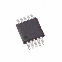
EL7515IY-T7 Intersil, EL7515IY-T7 Datasheet - Page 8

EL7515IY-T7
Manufacturer Part Number
EL7515IY-T7
Description
IC REG PWM STEP-UP 10-MSOP
Manufacturer
Intersil
Type
Step-Up (Boost)r
Datasheet
1.EL7515IYZ.pdf
(9 pages)
Specifications of EL7515IY-T7
Internal Switch(s)
Yes
Synchronous Rectifier
No
Number Of Outputs
1
Voltage - Output
4.5 ~ 17 V
Current - Output
600mA
Frequency - Switching
670kHz
Voltage - Input
1.8 ~ 13.2 V
Operating Temperature
-40°C ~ 85°C
Mounting Type
Surface Mount
Package / Case
10-MSOP, Micro10™, 10-uMAX, 10-uSOP
Lead Free Status / RoHS Status
Contains lead / RoHS non-compliant
Power - Output
-
Available stocks
Company
Part Number
Manufacturer
Quantity
Price
The boost converter output voltage is determined by the
relationship in Equation 8:
where V
this data sheet.
RC Filter
The maximum voltage rating for the VDD pin is 12V and is
recommended to be about 10V for maximum efficiency to
drive the internal MOSFET. The series resistor R
filter connected to V
If V
where I
10Ω to 51Ω with C
Thermal Performance
The EL7515 uses a fused-lead package, which has a
reduced θ
+115°C/W on a two-layer board. Maximizing copper around
the ground pins will improve the thermal performance.
This chip also has internal thermal shut-down set at around
+135°C to protect the component.
V
R
OUT
4
O
=
is larger than 10V, then Equation 9 shows:
V
-------------------- -
=
O
DD
I
FB
DD
V
–
JA
FB
10
is shown in I
slightly changes with V
×
of +100°C/W on a four-layer board and
⎛
⎜
⎝
1
+
4
R
------ -
R
DD
2
1
= 0.1µF.
⎞
⎟
⎠
DD
can be utilized to reduce the voltage.
vs f
S
8
curve. Otherwise, R
DD
. The curve is shown in
4
in the RC
4
can be
(EQ. 9)
(EQ. 8)
EL7515
Layout Considerations
The layout is very important for the converter to function
properly. Power Ground ( ) and Signal Ground (
be separated to ensure that the high pulse current in the
Power Ground never interferes with the sensitive signals
connected to Signal Ground. They should only be connected
at one point.
The trace connected to pin 8 (FB) is the most sensitive trace.
It needs to be as short as possible and in a “quiet” place,
preferably between PGND or SGND traces.
In addition, the bypass capacitor connected to the VDD pin
needs to be as close to the pin as possible.
The heat of the chip is mainly dissipated through the SGND
pin. Maximizing the copper area around it is preferable. In
addition, a solid ground plane is always helpful for the EMI
performance.
The demo board is a good example of layout based on these
principles. Please refer to the EL7515 Application Brief for
the layout. http://www.intersil.com/data/tb/tb429.pdf
August 10, 2007
) should
FN7120.2


