LM3100MH/NOPB National Semiconductor, LM3100MH/NOPB Datasheet - Page 13

LM3100MH/NOPB
Manufacturer Part Number
LM3100MH/NOPB
Description
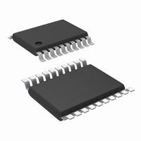
IC REG SIMPLE SW 1.5A 20-TSSOP
Manufacturer
National Semiconductor
Series
PowerWise®, SIMPLE SWITCHER®r
Type
Step-Down (Buck)r
Datasheet
1.LM3100MHXNOPB.pdf
(18 pages)
Specifications of LM3100MH/NOPB
Internal Switch(s)
Yes
Synchronous Rectifier
Yes
Number Of Outputs
1
Voltage - Output
0.8 ~ 7 V
Current - Output
1.5A
Frequency - Switching
1MHz
Voltage - Input
4.5 ~ 36 V
Operating Temperature
-40°C ~ 125°C
Mounting Type
Surface Mount
Package / Case
20-TSSOP Exposed Pad, 20-eTSSOP, 20-HTSSOP
Dc To Dc Converter Type
Step Down
Pin Count
20
Input Voltage
36V
Output Voltage
0.8 to 7V
Switching Freq
1000KHz
Output Current
1.5A
Efficiency
86%
Package Type
TSSOP EP
Output Type
Adjustable
Switching Regulator
Yes
Mounting
Surface Mount
Input Voltage (min)
4.5V
Operating Temp Range
-40C to 125C
Operating Temperature Classification
Automotive
For Use With
LM3100EVAL - BOARD EVAL LM3100
Lead Free Status / RoHS Status
Lead free / RoHS Compliant
Power - Output
-
Lead Free Status / Rohs Status
Compliant
Other names
*LM3100MH
*LM3100MH/NOPB
LM3100MH
*LM3100MH/NOPB
LM3100MH
N-Channel Buck Switch and Driver
The LM3100 integrates an N-Channel buck (high-side) switch
and associated floating high voltage gate driver. The gate
drive circuit works in conjunction with an external bootstrap
capacitor and an internal high voltage diode. A 33 nF capac-
itor (C
voltage to the high-side driver during the buck switch on-time.
During each off-time, the SW pin falls to approximately -1V
and C
diode. The minimum off-time of 260ns ensures adequate time
each cycle to recharge the bootstrap capacitor.
Soft-Start
The soft-start feature allows the converter to gradually reach
a steady state operating point, thereby reducing start-up
stresses and current surges. Upon turn-on, after V
the under-voltage threshold, an internal 8µA current source
charges up the external capacitor at the SS pin. The ramping
voltage at SS (and the non-inverting input of the regulation
comparator) ramps up the output voltage in a controlled man-
ner.
An internal switch grounds the SS pin if any of the following
cases happen: (i) VCC falls below the under-voltage lock-out
threshold; (ii) a thermal shutdown occurs; or (iii) the EN pin is
grounded. Alternatively, the converter can be disabled by
connecting the SS pin to ground using an external switch.
Releasing the switch allows the SS pin return to pull high and
the output voltage returns to normal. The shut-down configu-
ration is shown in
Thermal Protection
The LM3100 should be operated so the junction temperature
does not exceed the maximum limit. An internal Thermal
Shutdown circuit, which activates (typically) at 165°C, takes
the controller to a low power reset state by disabling the buck
switch and the on-timer, and grounding the SS pin. This fea-
ture helps prevent catastrophic failures from accidental de-
vice overheating. When the junction temperature falls back
below 145°C (typical hysteresis = 20°C), the SS pin is re-
leased and normal operation resumes.
Applications Information
EXTERNAL COMPONENTS
The following guidelines can be used to select the external
components.
R
FB1
FIGURE 3. Alternate Shutdown Implementation
and R
BST
BST
) connected between BST and SW pins provides
charges from the V
FB2
: The ratio of these resistors is calculated from:
Figure 3
.
CC
supply through the internal
20174706
CC
reaches
13
R
tors in the range of 1.0 kΩ - 10 kΩ which satisfy the above
ratio.
For V
directly. However, the converter operation needs a minimum
inductor current ripple to maintain good regulation when no
load is connected. This minimum load is about 10 µA and can
be implemented by adding a pre-load resistor to the output.
R
The equation 2 in Control Overview section can be used to
select R
above limitation is met.
L: The main parameter affected by the inductor is the output
current ripple amplitude (I
must be determined at both the minimum and maximum nom-
inal load currents. At minimum load current, the lower peak
must not reach 0A. At maximum load current, the upper peak
must not exceed the current limit threshold (1.9A). The allow-
able ripple current is calculated from the following equations:
or
The lesser of the two ripple amplitudes calculated above is
then used in the following equation:
where V
from equation 1. This provides a value for L. The next larger
standard value should be used. L should be rated for the I
current level shown in
FB1
ON
: The minimum value for R
and R
OUT
IN
ON
= 0.8V, the FB pin can be connected to the output
is the maximum input voltage and Fs is determined
FB2
if a specific frequency is desired as long as the
Inductor Selector for V
should be chosen from standard value resis-
I
OR(MAX2)
I
OR(MAX1)
Figure
= 2 x (1.9A - I
OR
). The maximum allowable (I
= 2 x I
2.
ON
is calculated from:
O(min)
OUT
O(max)
= 3.3V
)
20174736
www.national.com
(7)
OR
PK


